 ChipApex | Global Electronic Components Supplier
SEARCH
Search Product
Search Post
— IC芯片 | 连接器 | 传感器 | 被动器件 —
Search productSearch post
— IC芯片 | 连接器 | 传感器 | 被动器件 —
Consult the customer manager about the wholesale price.
consultation hotline:86-132-6715-2157
email:[email protected]
Contact the product manager for consultation. One-stop consultation is available.
Do you want a lower wholesale price? Please send us your inquiry and we will reply immediately.
The 5PB1203NTGK is a clock buffer integrated circuit manufactured by Renesas Electronics. It features one input and three outputs, operating at frequencies up to 200 MHz. The device supports an LVCMOS output format and functions within a supply voltage range of 1.71 V to 1.89 V. Maximum propagation delay is specified at 2.5 ns. It operates reliably between -40°C and +105°C. The component is housed in a 10-WFDFN package with an exposed pad, measuring 2.0 x 2.0 x 0.75 mm.
Verify the complete part number including suffixes such as 'T' or '8' when sourcing, as these may indicate specific tape-and-reel packaging or additive phase jitter specifications. Confirm that the supplier provides official documentation matching the 10-WFDFN package type. Ensure compatibility with the required 1.8V core voltage environment before integration into the design.
Select this component when a low-jitter, single-to-three fan-out clock buffer is required for LVCMOS applications. Consider the 200 MHz maximum frequency limit and 2.5 ns propagation delay for timing-sensitive designs. The exposed pad DFN package suits space-constrained surface-mount layouts requiring thermal dissipation capabilities.
This device belongs to the 5PB family of clock buffers from Renesas. It serves as a signal conditioning component for distributing reference clocks to multiple downstream loads. The technology utilizes advanced semiconductor processes to achieve low power consumption while maintaining signal integrity at high frequencies.
Publicly confirmed substitute part numbers are not available in the provided documentation. Verify pinout and electrical characteristics carefully if considering alternative vendors.
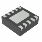 5PB1203NTGK
The activity of extra discounts on wholesale prices is in full swing…
Please fill in your contact information and we will send you the latest wholesale price list.





