 ChipApex | Global Electronic Components Supplier
SEARCH
Search Product
Search Post
— IC芯片 | 连接器 | 传感器 | 被动器件 —
Search productSearch post
— IC芯片 | 连接器 | 传感器 | 被动器件 —
Consult the customer manager about the wholesale price.
consultation hotline:86-132-6715-2157
email:[email protected]
Contact the product manager for consultation. One-stop consultation is available.
Do you want a lower wholesale price? Please send us your inquiry and we will reply immediately.
The 5PB1203NTGK8 is a mixed-signal clock buffer manufactured by Renesas Electronics. It features one input and three outputs, supporting a maximum frequency of 200 MHz. The device operates within a supply voltage range of 1.71 V to 1.89 V. It utilizes LVCMOS logic levels for both input and output signals. The component is housed in a 10-WFDFN exposed pad package with dimensions of 2.0 x 2.0 x 0.75 mm. It supports an operating temperature range from -40 °C to +105 °C.
Verify the specific suffix K8 against official Renesas documentation to confirm packaging details and reel specifications. Ensure compatibility with the required 10-WFDFN footprint and exposed pad thermal requirements during procurement. Confirm RoHS compliance status through current manufacturer declarations before finalizing orders.
Select this component when a single clock source requires splitting into three distinct paths with minimal skew. The 200 MHz capability suits moderate-speed digital applications. Verify that the 1.71 V to 1.89 V supply range aligns with the target system's voltage rails. Consider the DFN package size for PCB layout constraints.
This part belongs to the 5PB series of mixed-signal clock buffers from Renesas. It complements other variants like the 5PB1204 and 5PB1213, which offer different output counts or pin configurations. The series focuses on providing reliable clock distribution for embedded electronics requiring precise timing signals.
Direct substitutes include the 5PB1204CMGK8 for four-output applications. Check the 5PB1213NTGK8/H for alternative mixed-signal buffering needs. Always verify pinout compatibility and electrical specifications before swapping components.
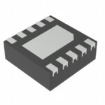 5PB1203NTGK8
The activity of extra discounts on wholesale prices is in full swing…
Please fill in your contact information and we will send you the latest wholesale price list.






