 ChipApex | Global Electronic Components Supplier
SEARCH
Search Product
Search Post
— IC芯片 | 连接器 | 传感器 | 被动器件 —
Search productSearch post
— IC芯片 | 连接器 | 传感器 | 被动器件 —
Consult the customer manager about the wholesale price.
consultation hotline:86-132-6715-2157
email:[email protected]
Contact the product manager for consultation. One-stop consultation is available.
Do you want a lower wholesale price? Please send us your inquiry and we will reply immediately.
The Renesas 5PB1204CMGK is a mixed-signal clock buffer featuring four outputs. It operates within a supply voltage range of 1.71 V to 1.89 V and supports maximum input frequencies up to 200 MHz. The device exhibits a maximum propagation delay of 2.5 ns. Designed for surface mount installation, it is housed in an 8-pin TSSOP package with dimensions of 3.1 x 4.4 x 1.0 mm. The component functions reliably across an extended temperature range from -40 °C to +105 °C.
Verify the specific suffix 'K' indicates cut tape packaging when sourcing. Confirm the 1.71 V to 1.89 V supply voltage constraint matches the target circuit design. Ensure the 8-pin TSSOP footprint aligns with the PCB layout requirements before procurement.
Select this component for designs requiring a single input to four output clock fan-out. The 5PB1204CMGK is suitable where low jitter and skew are critical. Verify that the system power rail can be regulated strictly between 1.71 V and 1.89 V to ensure proper operation.
This part belongs to the 5PB1204 series of high-performance clock buffers. It shares functional similarities with the 5PB1102 but provides four outputs instead of two. Both devices utilize similar LVCMOS technology and operate within comparable voltage ranges for clock distribution tasks.
The 5PB1102CMGK serves as a related alternative within the same product family. Note that the 5PB1102 offers only two outputs compared to the four outputs of the 5PB1204CMGK. Verify pin compatibility and output count requirements before substitution.
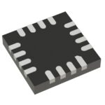 5PB1204CMGK
The activity of extra discounts on wholesale prices is in full swing…
Please fill in your contact information and we will send you the latest wholesale price list.






