ChipApex | Global Electronic Components Supplier
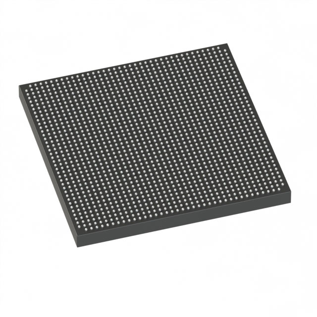
5SGSED8K1F40C2G
Search Product
Search Post
— IC芯片 | 连接器 | 传感器 | 被动器件 —
Search productSearch post
— IC芯片 | 连接器 | 传感器 | 被动器件 —
Consult the customer manager about the wholesale price.
consultation hotline:86-132-6715-2157
email:[email protected]
Contact the product manager for consultation. One-stop consultation is available.
Do you want a lower wholesale price? Please send us your inquiry and we will reply immediately.
The Altera 5SGSED8K1F40C2G is a Stratix V GS Field Programmable Gate Array (FPGA) designed for high-performance digital logic applications. It features 695,000 Logic Elements (LEs), organized into 26,240 Adaptive Logic Modules (ALMs) and 26,240 Logic Array Blocks (LABs). The device integrates 50 Mbits of embedded memory and supports up to 696 I/O pins. It operates within a supply voltage range of 0.9V and supports data rates up to 14.1 Gb/s via its integrated transceivers. The component is housed in a 1517-ball FCBGA package suitable for surface-mount assembly.
Verify the specific suffix 'C2G' against official Intel/Altera documentation to confirm temperature grade and packaging details. Confirm current production status as some Stratix V variants may be subject to lifecycle changes. Ensure compatibility with Quartus Prime software versions supporting the Stratix V family before procurement.
Select this model when designs require approximately 700k LEs and substantial embedded memory without the highest performance tier of the Stratix V GX or GT families. Compare against the 5SGXEA series if higher transceiver speeds are needed, or the 5SGSE series if lower logic density suffices. Verify power requirements against the 0.9V core voltage specification.
This part belongs to the Stratix V GS (General Speed) family, positioned between the standard Stratix V and the high-performance GX/GT variants. It shares the same 1517-FBGA footprint as other devices in the 5SGS...F40 form factor, facilitating potential pin-compatible upgrades or downgrades within the same package size.
Direct pin-to-pin replacements within the same package include the 5SGSED6K1F40C2G (lower capacity) or 5SGSED8N2F45C2LG (different package). Cross-family migration to Arria 10 or Cyclone V requires schematic redesign due to architectural differences.
 5SGSED8K1F40C2G
The activity of extra discounts on wholesale prices is in full swing…
Please fill in your contact information and we will send you the latest wholesale price list.