ChipApex | Global Electronic Components Supplier
5SGSED8K2F40I3N
Search Product
Search Post
— IC芯片 | 连接器 | 传感器 | 被动器件 —
Search productSearch post
— IC芯片 | 连接器 | 传感器 | 被动器件 —
Consult the customer manager about the wholesale price.
consultation hotline:86-132-6715-2157
email:[email protected]
Contact the product manager for consultation. One-stop consultation is available.
Do you want a lower wholesale price? Please send us your inquiry and we will reply immediately.
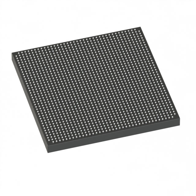
The Altera 5SGSED8K2F40I3N is a Stratix V GS Field Programmable Gate Array (FPGA) designed for high-density logic applications. It features 695,000 logic elements and 262,400 adaptive logic modules (ALMs). The device integrates 50 Mbit of embedded memory and supports data rates up to 14.1 Gb/s via its transceivers. Operating within a junction temperature range of 0°C to 85°C, it utilizes a 1517-ball FCBGA package with 696 I/Os. The core supply voltage operates between 0.82V and 0.88V.
Verify component authenticity through authorized channels due to the presence of counterfeit risks in the market. Confirm RoHS compliance status and moisture sensitivity level (MSL 3) prior to PCB assembly. Check for recent Product Change Notifications (PCNs) regarding labeling or packaging updates. Ensure proper handling procedures are followed to prevent electrostatic discharge damage during installation.
Select this model when high logic density is required without the need for high-speed GX transceivers found in the Stratix V GX series. Compare against the 5SGXED series if lower power consumption is critical. Verify that the 1517-ball package footprint matches the target PCB layout constraints. Ensure the design tool suite supports the specific Stratix V GS architecture.
This component belongs to the Stratix V GS family, which targets cost-sensitive, high-performance applications. It shares the same logical architecture as the Stratix V GX but omits the high-speed transceiver blocks to reduce cost and power. It serves as a bridge between the mid-range Stratix IV and the high-end Stratix V GX families.
Direct pin-to-pin replacements are not publicly documented for this specific part number. Consider the 5SGXED series for functional equivalence with added transceiver capabilities, though package and pinout differences may require redesign. Consult official distributor databases for end-of-life alternatives.
 5SGSED8K2F40I3N
The activity of extra discounts on wholesale prices is in full swing…
Please fill in your contact information and we will send you the latest wholesale price list.