ChipApex | Global Electronic Components Supplier
5SGSMD5K2F40I2N
Search Product
Search Post
— IC芯片 | 连接器 | 传感器 | 被动器件 —
Search productSearch post
— IC芯片 | 连接器 | 传感器 | 被动器件 —
Consult the customer manager about the wholesale price.
consultation hotline:86-132-6715-2157
email:[email protected]
Contact the product manager for consultation. One-stop consultation is available.
Do you want a lower wholesale price? Please send us your inquiry and we will reply immediately.
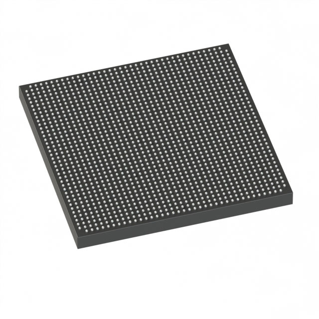
The Altera 5SGSMD5K2F40I2N is a Stratix V GS Field Programmable Gate Array featuring 457,000 logic elements and 172,600 adaptive logic modules. It integrates 39 Mbit of embedded memory and supports up to 696 I/Os within a 1517-ball FCBGA package. The device operates with supply voltages ranging from 0.87V to 0.93V and includes 36 transceivers capable of data rates up to 14.1 Gb/s. It is designed for surface mount applications across an operating temperature range of -40°C to 100°C.
This component is classified as obsolete and is no longer manufactured by Altera. Verification of part authenticity and condition is critical when sourcing from secondary markets. Buyers should confirm the specific suffix details against official datasheets to ensure functional compatibility, as legacy stock may vary in handling history or packaging integrity. Direct procurement from the manufacturer is not possible.
Engineers selecting this FPGA should evaluate the trade-off between the 457,000 logic element capacity and the available embedded memory blocks for their specific algorithm requirements. The 1517-ball package size and pin count must be accommodated within the PCB layout constraints. Designers must account for the specialized power delivery network required for the core voltage range and ensure adequate cooling solutions are integrated to maintain junction temperatures within the specified operational limits during peak activity.
The 5SGSMD5K2F40I2N belongs to the Stratix V GS family, representing a mid-range density option within the broader Stratix V portfolio. This series was engineered using 28-nm technology to provide a balance of performance, power efficiency, and cost-effectiveness for complex digital designs. The GS variant typically targets general-purpose high-volume applications requiring reliable programmable logic capabilities without the extreme density of top-tier models.
Public documentation identifies the 5SGSMD5K2F40I2G as a direct substitute for the 5SGSMD5K2F40I2N. Users should verify that the suffix change does not alter electrical characteristics or package specifications before implementation. Alternative migration paths may involve newer Intel Agilex or Arria families, though these require significant design re-verification due to architectural differences.


 5SGSMD5K2F40I2N
The activity of extra discounts on wholesale prices is in full swing…
Please fill in your contact information and we will send you the latest wholesale price list.