ChipApex | Global Electronic Components Supplier
5SGSMD5K3F40C3NCV
Search Product
Search Post
— IC芯片 | 连接器 | 传感器 | 被动器件 —
Search productSearch post
— IC芯片 | 连接器 | 传感器 | 被动器件 —
Consult the customer manager about the wholesale price.
consultation hotline:86-132-6715-2157
email:[email protected]
Contact the product manager for consultation. One-stop consultation is available.
Do you want a lower wholesale price? Please send us your inquiry and we will reply immediately.
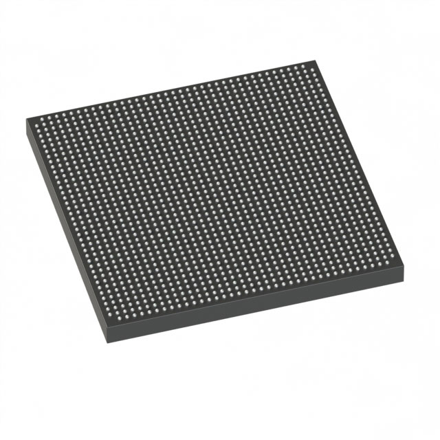
The Altera 5SGSMD5K3F40C3NCV is a Stratix V GS Field Programmable Gate Array featuring 457,000 logic elements and 172,600 adaptive logic modules. It integrates 39 Mbit of embedded memory across 17,260 LABs. The device supports data rates up to 14.1 Gb/s via its transceivers and operates with a core voltage of 850 mV. Designed for surface-mount installation in an FBGA-1517 package, it functions within a commercial temperature range of 0°C to +70°C.
Verify the exact suffix designation against official manufacturer documentation, as standard listings often utilize C2 or I3 variants rather than C3. Confirm current lifecycle status, as many Stratix V components are marked as obsolete or end-of-life. Ensure compatibility with legacy design tools and validate supply chain authenticity due to limited new production availability.
Select this component when high logic density and significant embedded memory are required within a commercial temperature environment. Compare against the 5SGSMD5K series for pin-compatible alternatives if specific I/O counts differ. Evaluate power consumption profiles relative to the Stratix V GX family for applications requiring higher speed but tolerating different thermal constraints.
This part belongs to the Stratix V GS family, targeting cost-sensitive applications requiring substantial logic resources. It shares architectural similarities with other 5SGSD5 devices but offers specific configuration parameters. The F40 designation indicates the 40mm package size, while the suffix defines temperature grade and speed binning.


 5SGSMD5K3F40C3NCV
The activity of extra discounts on wholesale prices is in full swing…
Please fill in your contact information and we will send you the latest wholesale price list.