ChipApex | Global Electronic Components Supplier
5SGSMD6K3F40C2LNCV
Search Product
Search Post
— IC芯片 | 连接器 | 传感器 | 被动器件 —
Search productSearch post
— IC芯片 | 连接器 | 传感器 | 被动器件 —
Consult the customer manager about the wholesale price.
consultation hotline:86-132-6715-2157
email:[email protected]
Contact the product manager for consultation. One-stop consultation is available.
Do you want a lower wholesale price? Please send us your inquiry and we will reply immediately.
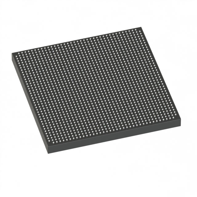
The Altera 5SGSMD6K3F40C2LG is a Stratix V GS Field Programmable Gate Array featuring 583,000 logic elements and 220,000 Adaptive Logic Modules. It integrates 46,080,000 total RAM bits and supports 696 I/Os within a 1517-ball FCBGA package. The device operates at a supply voltage of 0.82V to 0.88V and functions across a junction temperature range of 0°C to 85°C.
Verify the specific suffix codes against official manufacturer documentation to confirm exact electrical characteristics and environmental ratings. Ensure compatibility with required design tools and licensing models before procurement. Confirm RoHS compliance status through current datasheets as specifications may evolve.
Select this component for designs requiring high logic density and substantial on-chip memory bandwidth. Evaluate thermal management requirements given the power consumption profile of the Stratix V GS family. Ensure the PCB layout accommodates the large ball grid array footprint and signal integrity needs for high-speed interfaces.
This part belongs to the Stratix V GS series, targeting cost-sensitive high-performance applications. It offers a balance of logic capacity and memory depth suitable for mid-to-high complexity digital designs. The series is known for robust performance in industrial and communication sectors.
Publicly confirmed direct substitutes are not available in the provided source material. Consider reviewing newer Intel FPGA families for pin-compatible or functionally equivalent alternatives if end-of-life status applies. Verify architectural differences when migrating to other programmable logic devices.

 5SGSMD6K3F40C2LNCV
The activity of extra discounts on wholesale prices is in full swing…
Please fill in your contact information and we will send you the latest wholesale price list.