 ChipApex | Global Electronic Components Supplier
5SGXEA3K1F35C2LN
Search Product
Search Post
— IC芯片 | 连接器 | 传感器 | 被动器件 —
Search productSearch post
— IC芯片 | 连接器 | 传感器 | 被动器件 —
Consult the customer manager about the wholesale price.
consultation hotline:86-132-6715-2157
email:[email protected]
Contact the product manager for consultation. One-stop consultation is available.
Do you want a lower wholesale price? Please send us your inquiry and we will reply immediately.
The Altera 5SGXEA3K1F35C2LN is a Stratix V GX Field Programmable Gate Array (FPGA) designed for high-performance digital logic applications. It features 340,000 Logic Elements and 128,300 Adaptive Logic Modules within an FBGA-1152 package. The device includes 36 transceivers capable of data rates up to 14.1 Gb/s. Embedded memory totals 22.92 Mbit, comprising 19 Mbit of embedded RAM. It supports 432 I/Os and operates at a core voltage of 900 mV. The component is rated for commercial temperature ranges from 0°C to +70°C.
Verify the exact suffix configuration against official datasheets to ensure compatibility with specific voltage and temperature requirements. Confirm current lifecycle status as distribution availability varies. Check for moisture sensitivity handling procedures prior to assembly. Validate pinout definitions against the specific package variant to prevent integration errors during PCB design.
Compare total logic capacity and transceiver counts against system bandwidth requirements. Evaluate power consumption profiles at target operating frequencies. Ensure the FBGA-1152 footprint matches existing board layouts or allows for redesign. Consider thermal management solutions given the density of logic elements and active transceivers in this form factor.
This component belongs to the Stratix V GX family, which emphasizes high-speed serial connectivity. It shares the 1152-pin FBGA package with other variants in the series but differs in logic density and transceiver quantity. The 'GX' designation indicates optimized performance for serial communication interfaces compared to GS or GT families.
Direct substitutes are limited due to specific logic and transceiver configurations. Review other Stratix V GX parts with similar I/O counts and transceiver numbers. Verify pin-to-pin compatibility if replacing within the same package type. Consult manufacturer obsolescence notices for recommended migration paths.
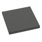 5SGXEA3K1F35C2LN
The activity of extra discounts on wholesale prices is in full swing…
Please fill in your contact information and we will send you the latest wholesale price list.





