ChipApex | Global Electronic Components Supplier
5SGXEA3K1F40C2N
Search Product
Search Post
— IC芯片 | 连接器 | 传感器 | 被动器件 —
Search productSearch post
— IC芯片 | 连接器 | 传感器 | 被动器件 —
Consult the customer manager about the wholesale price.
consultation hotline:86-132-6715-2157
email:[email protected]
Contact the product manager for consultation. One-stop consultation is available.
Do you want a lower wholesale price? Please send us your inquiry and we will reply immediately.
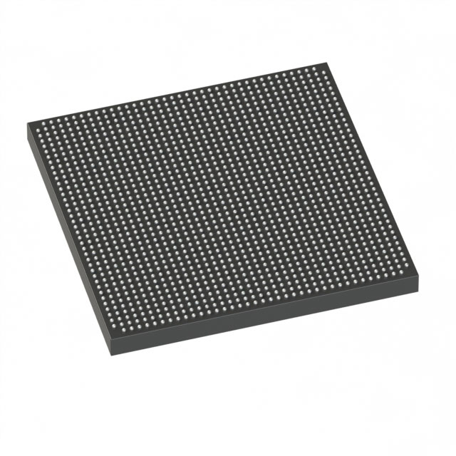
The Altera 5SGXEA3K1F40C2N is a Stratix V GX Field Programmable Gate Array featuring 340,000 logic elements and 128,300 adaptive logic modules. It integrates 19 Mbit of embedded memory within 12,830 LABs and supports up to 696 I/Os. The device includes 36 transceivers capable of 14.1 Gb/s data rates. Operating at a core voltage of 850 mV, it functions within a commercial temperature range of 0°C to +70°C. The component is housed in a 1517-pin FBGA package.
Verify the exact suffix configuration against official datasheets to ensure correct temperature grade and package variant. Confirm current lifecycle status as distribution channels may list obsolete inventory. Validate RoHS compliance documentation prior to integration into regulated assemblies.
Compare total logic element counts and transceiver bandwidth requirements against alternative Stratix V variants. Ensure the selected package pinout matches the target PCB layout constraints. Verify that the available embedded memory meets system buffering needs without external components.
This component belongs to the Stratix V GX family, designed for high-speed serial applications. It shares architectural similarities with other 5SGX models but offers specific resource scaling. The part represents a mid-range density option within the broader FPGA portfolio.
Consult official cross-reference guides for direct pin-compatible upgrades within the Stratix V series. Verify functional equivalence for transceiver specifications when considering higher-density alternatives.
 5SGXEA3K1F40C2N
The activity of extra discounts on wholesale prices is in full swing…
Please fill in your contact information and we will send you the latest wholesale price list.