ChipApex | Global Electronic Components Supplier
5SGXEA4K3F40C2L
Search Product
Search Post
— IC芯片 | 连接器 | 传感器 | 被动器件 —
Search productSearch post
— IC芯片 | 连接器 | 传感器 | 被动器件 —
Consult the customer manager about the wholesale price.
consultation hotline:86-132-6715-2157
email:[email protected]
Contact the product manager for consultation. One-stop consultation is available.
Do you want a lower wholesale price? Please send us your inquiry and we will reply immediately.
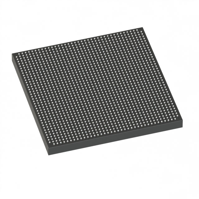
The Altera 5SGXEA4K3F40C2L is a Stratix V GX Field Programmable Gate Array (FPGA) featuring 420,000 logic elements and 158,500 Adaptive Logic Modules. It includes 37 Mbit of embedded memory and supports 696 I/Os within a 1517-pin FBGA package. The device operates at a core voltage of 850 mV with a maximum data rate of 14.1 Gb/s across 36 transceivers. It functions within a commercial temperature range of 0°C to +70°C.
This component is officially designated as obsolete by the manufacturer and is no longer in active production. Verification of availability should focus on authorized distributors holding remaining stock or certified third-party suppliers offering compatible alternatives. Buyers must confirm authenticity and storage conditions due to the part's end-of-life status.
Engineers selecting this FPGA should evaluate its specific 1517-pin FBGA footprint and 696 I/O count against current design requirements. The Stratix V GX architecture offers distinct advantages for high-speed serial applications compared to lower-tier families. Designers must account for the device's thermal characteristics and power supply stability given the 850 mV core voltage operation.
Belonging to the Stratix V GX family, this FPGA targets performance-intensive applications requiring robust serial connectivity. The series combines high-density logic with specialized transceiver blocks, making it suitable for demanding digital signal processing and interface conversion roles within enterprise and industrial hardware ecosystems.
The direct substitute part number is 5SGXEA4K3F40C2LG.
The device supports a maximum data rate of 14.1 Gb/s via its integrated transceivers.
The component contains 36 high-speed serial transceivers.


 5SGXEA4K3F40C2L
The activity of extra discounts on wholesale prices is in full swing…
Please fill in your contact information and we will send you the latest wholesale price list.