 ChipApex | Global Electronic Components Supplier
5SGXEA5K1F40I2G
Search Product
Search Post
— IC芯片 | 连接器 | 传感器 | 被动器件 —
Search productSearch post
— IC芯片 | 连接器 | 传感器 | 被动器件 —
Consult the customer manager about the wholesale price.
consultation hotline:86-132-6715-2157
email:[email protected]
Contact the product manager for consultation. One-stop consultation is available.
Do you want a lower wholesale price? Please send us your inquiry and we will reply immediately.
The Altera 5SGXEA5K1F40I2G is a Stratix V GX Field Programmable Gate Array (FPGA) featuring 490,000 logic elements and 185,000 adaptive logic modules. It integrates 36 transceivers capable of data rates up to 14.1 Gb/s and includes 50.65 Mbit of total embedded memory. The device operates within a junction temperature range of -40°C to 100°C and utilizes an 850 mV core voltage. Packaged in a 1517-ball FCBGA with 696 I/Os, it supports surface-mount installation and meets RoHS compliance standards.
Verify component authenticity through authorized distribution channels due to the prevalence of counterfeit integrated circuits. Confirm that the specific suffix indicates the intended industrial temperature rating and package variant. Ensure handling procedures account for moisture sensitivity levels to prevent damage during assembly. Cross-reference datasheet revisions to confirm current manufacturing status and availability constraints.
Compare against other Stratix V GX variants based on required logic density and transceiver count. Evaluate power consumption profiles relative to available cooling solutions. Verify pin compatibility if replacing existing designs. Consider long-term supply chain stability given the product lifecycle stage. Assess software toolchain support requirements for Quartus Prime implementation.
This component belongs to the Stratix V GX family, designed for high-performance serial communication applications. It shares architectural similarities with other devices in the 5SGX series but offers specific resource configurations tailored for bandwidth-intensive tasks. The part represents a generation of FPGAs bridging mid-range and high-end market segments.
Direct substitutes include other Stratix V GX parts with matching pinouts and comparable logic resources, such as the 5SGXEA5K1F40C2L or 5SGXMA5K2F40I3LG. Verify functional equivalence regarding transceiver capabilities and memory sizes before integration into existing hardware designs.
The integrated transceivers support data rates up to 14.1 Gb/s.
Yes, the device is rated for junction temperatures ranging from -40°C to 100°C.
The component provides a total of 50.65 Mbit of embedded memory resources.
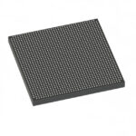 5SGXEA5K1F40I2G
The activity of extra discounts on wholesale prices is in full swing…
Please fill in your contact information and we will send you the latest wholesale price list.





