 ChipApex | Global Electronic Components Supplier
5SGXEA5K3F40C2L
Search Product
Search Post
— IC芯片 | 连接器 | 传感器 | 被动器件 —
Search productSearch post
— IC芯片 | 连接器 | 传感器 | 被动器件 —
Consult the customer manager about the wholesale price.
consultation hotline:86-132-6715-2157
email:[email protected]
Contact the product manager for consultation. One-stop consultation is available.
Do you want a lower wholesale price? Please send us your inquiry and we will reply immediately.
The Altera 5SGXEA5K3F40C2L is a Stratix V GX Field Programmable Gate Array (FPGA) designed for high-performance digital signal processing and networking applications. It features 490,000 logic elements and 185,000 adaptive logic modules within a 1517-ball FBGA package. The device includes 36 transceivers capable of data rates up to 14.1 Gb/s and provides 696 I/Os. Embedded memory totals 37 Mbit with a core operating voltage of 850 mV. It supports an industrial temperature range from 0°C to +70°C.
Verify component authenticity through authorized distribution channels due to the prevalence of counterfeits in the FPGA market. Confirm that the specific suffix indicates the correct temperature grade and package variant required for your design. Request full traceability documentation including lot codes and manufacturing dates to ensure compliance with quality standards. Check for any known obsolescence notices or lifecycle status updates from the manufacturer before finalizing procurement plans.
Compare this model against other Stratix V variants based on specific transceiver count requirements and total logic density needs. Ensure the 1517-ball package footprint matches your PCB layout constraints and thermal management strategy. Evaluate power consumption profiles under typical operating loads to verify compatibility with your power delivery network. Consider pinout compatibility if migrating from previous generation devices to minimize redesign efforts.
This component belongs to the Stratix V GX family, which emphasizes high-speed serial connectivity. It sits alongside other models like the 5SGXEA5N2F40C3G but differs in specific resource allocation and package options. The GX series is distinct from the GS and GT families by its focus on transceiver performance rather than pure logic density or low power consumption.
Direct pin-to-pin replacements are limited within the same family due to varying resource densities. Review the 5SGXEA5N2F40C3G for similar form factor but different internal configuration. Consult official migration guides for architectural differences when considering upgrades to Agilex or Stratix 10 families.


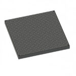 5SGXEA5K3F40C2L
The activity of extra discounts on wholesale prices is in full swing…
Please fill in your contact information and we will send you the latest wholesale price list.



