 ChipApex | Global Electronic Components Supplier
5SGXEA7H2F35I3
Search Product
Search Post
— IC芯片 | 连接器 | 传感器 | 被动器件 —
Search productSearch post
— IC芯片 | 连接器 | 传感器 | 被动器件 —
Consult the customer manager about the wholesale price.
consultation hotline:86-132-6715-2157
email:[email protected]
Contact the product manager for consultation. One-stop consultation is available.
Do you want a lower wholesale price? Please send us your inquiry and we will reply immediately.
The Altera 5SGXEA7H2F35I3 is a Stratix V GX Field Programmable Gate Array featuring 622,000 logic elements and 23,472 adaptive logic modules. It integrates 50 Mbit of embedded memory and supports 552 I/Os within an FBGA-1152 package. The device operates at a core voltage of 900 mV with a maximum data rate of 14.1 Gb/s across 24 transceivers. It functions within a temperature range of -40°C to +85°C.
Verify component authenticity through authorized channels due to end-of-life status. Confirm RoHS compliance details as listed in official documentation. Check moisture sensitivity level handling requirements before assembly. Validate pinout compatibility with existing PCB layouts. Ensure design tools support the specific device variant.
Compare logic density and transceiver counts against project requirements. Evaluate power consumption profiles relative to thermal constraints. Assess memory bandwidth needs for data throughput applications. Consider package size limitations for board real estate. Verify software toolchain compatibility for development workflows.
This component belongs to the Stratix V GX family, designed for high-bandwidth applications requiring significant parallel processing capabilities. It represents a generation of FPGAs optimized for telecom and enterprise markets before subsequent product lines were introduced.
Publicly confirmed substitute part numbers are not available in the provided source material.

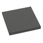 5SGXEA7H2F35I3
The activity of extra discounts on wholesale prices is in full swing…
Please fill in your contact information and we will send you the latest wholesale price list.




