 ChipApex | Global Electronic Components Supplier
5SGXEA9N2F45C2L
Search Product
Search Post
— IC芯片 | 连接器 | 传感器 | 被动器件 —
Search productSearch post
— IC芯片 | 连接器 | 传感器 | 被动器件 —
Consult the customer manager about the wholesale price.
consultation hotline:86-132-6715-2157
email:[email protected]
Contact the product manager for consultation. One-stop consultation is available.
Do you want a lower wholesale price? Please send us your inquiry and we will reply immediately.
The Altera 5SGXEA9N2F45C2L is a Stratix V GX Field Programmable Gate Array (FPGA) featuring 840 I/Os and housed in a 1932-BBGA, FCBGA package. It contains 840,000 logic elements, 317,000 Adaptive Logic Modules (ALMs), and 31,700 Logic Array Blocks (LABs). The device includes 52 Mbit of embedded memory and supports data rates up to 14.1 Gb/s via 48 transceivers. Operating voltage ranges from 0.87V to 0.93V, with an operating temperature range of 0°C to 85°C TJ.
Verify the specific suffix codes against official Intel/Altera documentation to ensure correct speed grade and temperature rating. Confirm RoHS compliance status and moisture sensitivity level requirements prior to ordering. Check for any recent Product Change Notifications regarding label or packaging updates. Ensure compatibility with required design tools and licensing models before finalizing procurement plans.
Select this component when high logic density and significant embedded memory are required alongside multiple high-speed serial interfaces. Evaluate power consumption profiles against available cooling solutions due to the dense integration. Consider the 1932-pin package dimensions for PCB layout constraints and thermal management strategies during the initial design phase.
This part belongs to the Stratix V GX family, designed for applications requiring high-performance logic and extensive connectivity. It represents a generation of FPGAs optimized for complex system integration and high-speed data handling within enterprise and industrial sectors.
Consult official substitution guides for compatible variants within the Stratix V series. Verify pinout and functional equivalence if considering alternative packages or speed grades.
The integrated transceivers support data rates up to 14.1 Gb/s.
The device includes 52 Mbit of embedded memory resources.
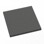 5SGXEA9N2F45C2L
The activity of extra discounts on wholesale prices is in full swing…
Please fill in your contact information and we will send you the latest wholesale price list.






