 ChipApex | Global Electronic Components Supplier
5SGXEA9N3F45I3L
Search Product
Search Post
— IC芯片 | 连接器 | 传感器 | 被动器件 —
Search productSearch post
— IC芯片 | 连接器 | 传感器 | 被动器件 —
Consult the customer manager about the wholesale price.
consultation hotline:86-132-6715-2157
email:[email protected]
Contact the product manager for consultation. One-stop consultation is available.
Do you want a lower wholesale price? Please send us your inquiry and we will reply immediately.
The Altera 5SGXEA9N3F45I3L is a Stratix V GX Field Programmable Gate Array (FPGA) featuring 840,000 logic elements and 317,000 adaptive logic modules. It integrates 52 Mbit of embedded memory and supports up to 840 I/Os within a 1932-pin FBGA package. The device includes 48 transceivers capable of data rates up to 14.1 Gb/s. Operating voltage is fixed at 850 mV, with an industrial temperature range spanning from -40°C to +85°C.
Verify component authenticity through authorized channels due to end-of-life status. Confirm moisture sensitivity level handling requirements during storage and assembly. Validate pinout compatibility with existing PCB layouts before procurement. Check for specific revision markings that may indicate manufacturing date codes or packaging variations.
Compare against other Stratix V GX variants based on required transceiver count and I/O density. Ensure the 1932-pin FBGA footprint matches available board space and thermal dissipation capabilities. Evaluate power supply design constraints given the fixed 850 mV core voltage requirement. Consider legacy support availability for Quartus Prime software versions compatible with this device family.
This component belongs to the Stratix V GX series, designed for high-bandwidth applications requiring significant parallel processing and serial interface capabilities. It represents a generation of FPGAs optimized for telecommunications and data center environments where throughput and latency are critical performance metrics.
Publicly confirmed substitute part numbers are not available in the provided documentation. Engineering change notices should be consulted for potential obsolescence management strategies or approved alternative devices within the same product family.

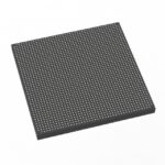 5SGXEA9N3F45I3L
The activity of extra discounts on wholesale prices is in full swing…
Please fill in your contact information and we will send you the latest wholesale price list.




