 ChipApex | Global Electronic Components Supplier
5SGXEABN3F45I3L
Search Product
Search Post
— IC芯片 | 连接器 | 传感器 | 被动器件 —
Search productSearch post
— IC芯片 | 连接器 | 传感器 | 被动器件 —
Consult the customer manager about the wholesale price.
consultation hotline:86-132-6715-2157
email:[email protected]
Contact the product manager for consultation. One-stop consultation is available.
Do you want a lower wholesale price? Please send us your inquiry and we will reply immediately.
The Altera 5SGXEABN3F45I3L is a Stratix V GX Field Programmable Gate Array (FPGA) belonging to the 5SGXA9 device family. It features 952,000 logic elements and 359,200 Adaptive Logic Modules (ALMs). The device includes 52 Mbit of embedded memory and supports up to 840 I/Os. It operates with a core voltage range of 0.82V to 0.88V and supports data rates up to 14.1 Gb/s via its transceivers. The component is housed in a 1932-ball FCBGA package and is rated for an operating temperature range of -40°C to +100°C.
Verify the specific suffix 'I3L' against official Altera documentation to confirm the exact temperature grade and package variant, as suffixes define critical environmental and mechanical specifications. Confirm RoHS compliance status and moisture sensitivity level requirements prior to integration into surface-mount assembly processes.
Select this model when design requirements exceed the capacity of lower-density Stratix V devices but do not necessitate the higher performance of Stratix V GT or GX variants with different transceiver counts. Ensure the 1932-ball package footprint fits within the board layout constraints and that the thermal solution can handle the power dissipation associated with 952,000 logic elements.
This component is part of the Stratix V GX family, designed for applications requiring high bandwidth and significant logic density. It represents a generation of FPGAs optimized for cost-effective high-performance computing and connectivity solutions before subsequent Agilex architectures were introduced.
Direct pin-to-pin replacements are generally unavailable due to architectural differences between FPGA generations. Migration typically requires redesigning the PCB and updating the Quartus Prime design files to target a newer device family such as Agilex or Stratix 10.
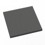 5SGXEABN3F45I3L
The activity of extra discounts on wholesale prices is in full swing…
Please fill in your contact information and we will send you the latest wholesale price list.






