ChipApex | Global Electronic Components Supplier

SEARCH
Search Product
Search Post
— IC芯片 | 连接器 | 传感器 | 被动器件 —
Search productSearch post
— IC芯片 | 连接器 | 传感器 | 被动器件 —
Consult the customer manager about the wholesale price.
consultation hotline:86-132-6715-2157
email:[email protected]
Contact the product manager for consultation. One-stop consultation is available.
Do you want a lower wholesale price? Please send us your inquiry and we will reply immediately.
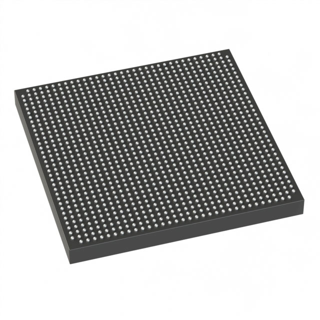
5SGXMA3H1F35C2WN is listed in the Field Programmable Gate Array range at ChipApex. The manufacturer field lists Altera. Its product description is IC FPGA 600 I/O 1152FBGA. Review the specifications below when checking this part for your BOM.
The Altera 5SGXMA3H1F35C2WN is a Stratix V GX Field Programmable Gate Array featuring 340,000 logic elements and 128,300 Adaptive Logic Modules. It includes 19 Mbit of embedded memory and supports up to 600 I/Os within a 1152-ball FCBGA package. The device operates at a supply voltage of 0.87V to 0.93V with a maximum data rate of 14.1 Gb/s across its transceivers.
Verify component authenticity through authorized channels due to potential availability constraints. Confirm RoHS compliance and moisture sensitivity level requirements prior to assembly. Ensure storage conditions meet JEDDEC standards to prevent damage before reflow soldering processes are initiated.
Evaluate the specific requirement for 14.1 Gb/s transceiver speeds against alternative Stratix V variants. Consider the 1152-ball package footprint constraints during PCB layout planning. Assess thermal management needs given the high logic density and power consumption characteristics inherent to this FPGA family.
This component belongs to the Stratix V GX series, designed for high-performance applications requiring substantial parallel processing capabilities. It utilizes Intel's advanced manufacturing process to deliver high logic density within a compact form factor suitable for demanding electronic systems.
Public confirmed substitute part numbers are not available in the provided documentation. Verify compatibility with existing design files when considering alternative FPGA families or updated generation devices from the manufacturer.
Explore related parts through Embedded, Integrated Circuits (ICs), all product categories, ChipApex homepage.
 5SGXMA3H1F35C2WN

5SGXMA3H1F35C2WN is listed in the Field Programmable Gate Array range at ChipApex. The manufacturer field lists Altera. Its product description is IC FPGA 600…
Read More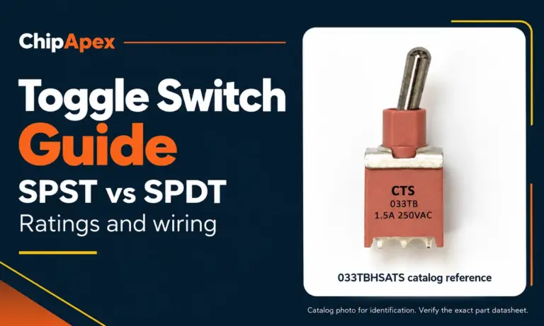
Compare SPST and SPDT toggle switches, understand AC/DC ratings, and follow wiring examples. Check contact action, mounting and parts in the ChipApex catalog.
Read More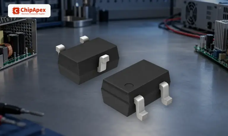
Learn how a diode conducts, how to identify anode and cathode, and when to choose rectifier, TVS, Zener or photodiode types for a circuit.
Read More
5SGXMA3H1F35C2WN is listed in the Field Programmable Gate Array range at ChipApex. The manufacturer field lists Altera. Its product description is IC FPGA 600…
Read More
Learn what an IMU measures, how accelerometers and gyroscopes work together, why orientation estimates drift, and what to compare.
Read More
5SGXMA3H1F35C2WN is listed in the Field Programmable Gate Array range at ChipApex. The manufacturer field lists Altera. Its product description is IC FPGA 600…
Read More
5SGXMA3H1F35C2WN is listed in the Field Programmable Gate Array range at ChipApex. The manufacturer field lists Altera. Its product description is IC FPGA 600…
Read More
Select MOV varistors by continuous voltage, clamping behavior, surge waveform and repetition. Check thermal disconnection, fuse coordination and replacements.
Read More
5SGXMA3H1F35C2WN is listed in the Field Programmable Gate Array range at ChipApex. The manufacturer field lists Altera. Its product description is IC FPGA 600…
Read More
5SGXMA3H1F35C2WN is listed in the Field Programmable Gate Array range at ChipApex. The manufacturer field lists Altera. Its product description is IC FPGA 600…
Read More
5SGXMA3H1F35C2WN is listed in the Field Programmable Gate Array range at ChipApex. The manufacturer field lists Altera. Its product description is IC FPGA 600…
Read More
5SGXMA3H1F35C2WN is listed in the Field Programmable Gate Array range at ChipApex. The manufacturer field lists Altera. Its product description is IC FPGA 600…
Read More
The activity of extra discounts on wholesale prices is in full swing…
Please fill in your contact information and we will send you the latest wholesale price list.