 ChipApex | Global Electronic Components Supplier

SEARCH
Search Product
Search Post
— IC芯片 | 连接器 | 传感器 | 被动器件 —
Search productSearch post
— IC芯片 | 连接器 | 传感器 | 被动器件 —
Consult the customer manager about the wholesale price.
consultation hotline:86-132-6715-2157
email:[email protected]
Contact the product manager for consultation. One-stop consultation is available.
Do you want a lower wholesale price? Please send us your inquiry and we will reply immediately.
5SGXMA9N2F45I2LG is listed in the Field Programmable Gate Array range at ChipApex. The manufacturer field lists Altera. Its product description is IC FPGA 840 I/O 1932FCBGA. Review the specifications below when checking this part for your BOM.
The Altera 5SGXMA9N2F45I2LG is a Stratix V GX Field Programmable Gate Array (FPGA) featuring 840 I/Os and housed in a 1932-BBGA, FCBGA package. It contains 840,000 logic elements, 31,700 LABs/CLBs, and 62.96 Mbits of total embedded memory. The device operates within a supply voltage range of 0.82V to 0.88V and supports a data rate of 14.1 Gb/s across its transceivers. It functions reliably within a junction temperature range of -40°C to 100°C.
Verify the exact suffix against official Intel/Altera documentation to confirm specific binning or environmental ratings. Confirm RoHS compliance status directly with the manufacturer as regulatory statuses can change. Ensure the ordering part number matches the required package and temperature grade specifications precisely before finalizing procurement orders.
Select this component when high-density logic capacity combined with significant embedded memory is required for complex digital signal processing. The Stratix V GX series is suitable for applications demanding high-speed serial interfaces and robust on-chip interconnectivity. Evaluate power consumption profiles against available cooling solutions given the dense integration.
This FPGA belongs to the Stratix V GX family, designed for high-performance computing and networking applications. The series emphasizes advanced transceiver technology and extensive memory resources. It serves as a foundational component for developing sophisticated electronic systems requiring reconfigurable hardware acceleration and flexible interface capabilities.
Public confirmed substitute part numbers are not available in the provided source material.
Explore related parts through Embedded, Integrated Circuits (ICs), all product categories, ChipApex homepage.


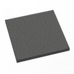 5SGXMA9N2F45I2LG

The activity of extra discounts on wholesale prices is in full swing…
Please fill in your contact information and we will send you the latest wholesale price list.




