 ChipApex | Global Electronic Components Supplier

SEARCH
Search Product
Search Post
— IC芯片 | 连接器 | 传感器 | 被动器件 —
Search productSearch post
— IC芯片 | 连接器 | 传感器 | 被动器件 —
Consult the customer manager about the wholesale price.
consultation hotline:86-132-6715-2157
email:[email protected]
Contact the product manager for consultation. One-stop consultation is available.
Do you want a lower wholesale price? Please send us your inquiry and we will reply immediately.
5SGXMA9N2F45I2LN is listed in the Field Programmable Gate Array range at ChipApex. The manufacturer field lists Altera. Its product description is IC FPGA 840 I/O 1932FBGA. Review the specifications below when checking this part for your BOM.
The Altera 5SGXMA9N2F45I2LN is a Stratix V GX Field Programmable Gate Array (FPGA) designed for high-performance digital logic applications. It features 1,064,000 logic elements and 401,280 adaptive logic modules within its architecture. The device includes 52 Mbit of embedded memory and supports up to 840 I/O pins. It integrates 48 transceivers capable of data rates up to 14.1 Gb/s. Operating at a core voltage of 850 mV, it functions within an industrial temperature range of -40°C to +100°C. The component is housed in a 1932-ball FBGA package.
Verify the specific suffix codes against official Intel/Altera documentation to confirm temperature grade and package variations. Confirm end-of-life status or obsolescence notices prior to design finalization. Ensure supply chain sources provide valid traceability for sensitive electronic components.
Compare logic element counts and transceiver specifications against alternative Stratix V variants to ensure adequate resource headroom. Evaluate power consumption profiles relative to available thermal management solutions. Verify compatibility with existing Quartus Prime software versions for design implementation.
This component belongs to the Stratix V GX family, which emphasizes high-speed serial connectivity alongside significant logic density. It serves as a successor to previous generations, offering enhanced performance per watt for demanding digital signal processing tasks.
Consult official Intel cross-reference tools for verified equivalent part numbers. Consider newer Agilex series devices for improved performance metrics if form-factor constraints allow.
Explore related parts through Embedded, Integrated Circuits (ICs), all product categories, ChipApex homepage.
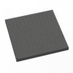 5SGXMA9N2F45I2LN

The activity of extra discounts on wholesale prices is in full swing…
Please fill in your contact information and we will send you the latest wholesale price list.





