 ChipApex | Global Electronic Components Supplier

SEARCH
Search Product
Search Post
— IC芯片 | 连接器 | 传感器 | 被动器件 —
Search productSearch post
— IC芯片 | 连接器 | 传感器 | 被动器件 —
Consult the customer manager about the wholesale price.
consultation hotline:86-132-6715-2157
email:[email protected]
Contact the product manager for consultation. One-stop consultation is available.
Do you want a lower wholesale price? Please send us your inquiry and we will reply immediately.
5SGXMABK3H40C2LN is listed in the Field Programmable Gate Array range at ChipApex. The manufacturer field lists Altera. Its product description is IC FPGA 696 I/O 1517HBGA. Review the specifications below when checking this part for your BOM.
The Altera 5SGXMABK3H40C2LN is a Stratix V GX Field Programmable Gate Array (FPGA) featuring 952,000 logic elements and 359,200 Adaptive Logic Modules. It integrates 52 Mbit of embedded memory and provides 696 I/Os. The device operates at a supply voltage of 850 mV and supports data rates up to 14.1 Gb/s via 36 transceivers. It is housed in a 1517-pin FineLine BGA package with an operating temperature range of 0°C to +70°C.
Verify component authenticity through authorized distributors or direct manufacturer channels due to potential availability constraints. Confirm RoHS compliance status and moisture sensitivity level prior to procurement. Ensure storage conditions meet specified humidity thresholds to prevent damage before soldering.
Evaluate thermal management requirements carefully as the device generates significant heat during operation. Verify that the PCB layout accommodates the 1517-pin FCBGA footprint and associated power delivery network specifications. Ensure compatibility with Quartus Prime design software versions supporting this specific Stratix V family member.
This component belongs to the Stratix V GX family, designed for high-performance computing and communications markets. It represents a mature generation of FPGA technology from Altera, now part of Intel, offering a balance of performance and resource density for demanding digital logic implementations.
Direct pin-to-pin replacements are not publicly documented for this specific suffix combination. Consider evaluating newer Intel Agilex or Stratix 10 families for functional equivalents, though architectural differences require comprehensive redesign. Consult official Intel documentation for legacy support guidelines.
Explore related parts through Embedded, Integrated Circuits (ICs), all product categories, ChipApex homepage.


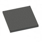 5SGXMABK3H40C2LN

The activity of extra discounts on wholesale prices is in full swing…
Please fill in your contact information and we will send you the latest wholesale price list.



