 ChipApex | Global Electronic Components Supplier
SEARCH
Search Product
Search Post
— IC芯片 | 连接器 | 传感器 | 被动器件 —
Search productSearch post
— IC芯片 | 连接器 | 传感器 | 被动器件 —
Consult the customer manager about the wholesale price.
consultation hotline:86-132-6715-2157
email:[email protected]
Contact the product manager for consultation. One-stop consultation is available.
Do you want a lower wholesale price? Please send us your inquiry and we will reply immediately.
The Renesas 5T30553DCGI8 is a low skew clock buffer featuring one input and four outputs. It operates within a supply voltage range of 2.5V to 3.3V and supports maximum input frequencies up to 200 MHz. The device guarantees extremely low output skew with a maximum value of 50 ps. It utilizes low power CMOS technology and is housed in an 8-pin SOIC package. The component is designed for surface mount installation and functions reliably across an operating temperature range from -40°C to +85°C.
Verify the specific suffix GI8 confirms the 8-pin SOIC package configuration and RoHS compliance status before procurement. Confirm that the required operating temperature range aligns with the specified -40°C to +85°C limits. Ensure design compatibility with the 2.5V or 3.3V core voltage requirements. Check current availability as this part may be subject to obsolescence notices.
Select this component when minimal clock skew is critical for system synchronization. It is suitable for applications requiring a single source to drive multiple loads with tight timing constraints. Consider the 8-pin SOIC package size for PCB layout constraints. Verify that the LVCMOS input type matches the driving source logic levels.
This component belongs to the 5T30553 series of clock buffers manufactured by Renesas Electronics. It is designed to provide reliable fanout buffering for high-frequency clock signals. The series is characterized by its ability to maintain signal integrity across multiple output branches while minimizing timing variations between channels.
Public confirmed substitute part numbers are not available in the provided documentation.
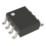 5T30553DCGI8
The activity of extra discounts on wholesale prices is in full swing…
Please fill in your contact information and we will send you the latest wholesale price list.






