 ChipApex | Global Electronic Components Supplier
SEARCH
Search Product
Search Post
— IC芯片 | 连接器 | 传感器 | 被动器件 —
Search productSearch post
— IC芯片 | 连接器 | 传感器 | 被动器件 —
Consult the customer manager about the wholesale price.
consultation hotline:86-132-6715-2157
email:[email protected]
Contact the product manager for consultation. One-stop consultation is available.
Do you want a lower wholesale price? Please send us your inquiry and we will reply immediately.
The 5T9050PGGI is a single-ended input to five single-ended outputs clock buffer built on advanced metal CMOS technology. It operates as a 2.5V single data rate (SDR) device with a maximum frequency of 200 MHz. The supply voltage range is 2.3V to 2.7V. The component is housed in a 28-TSSOP package, measuring 4.40mm in width. This specific part number is currently classified as obsolete.
Verify the obsolete status of this component before procurement planning. Confirm availability through authorized distributors or secondary market sources. Ensure compatibility with existing 2.5V SDR designs. Check for lead time variations due to limited stock. Validate pinout and package dimensions against current board layouts.
Select this component for designs requiring a 1:5 LVCMOS/LVTTL fanout buffer. Consider the 28-TSSOP package constraints. Evaluate the 2.3V to 2.7V supply requirement. Assess the 200 MHz maximum frequency limit. Note the obsolete status may impact long-term production viability.
This part belongs to the 5T9050 series of clock buffers from Renesas Electronics. The series focuses on single-ended clock distribution using metal CMOS processes. The PGGI suffix indicates the specific package type and temperature grade within the product line.
Public confirmed substitute part numbers are not available in the provided documentation. Due to the obsolete status, alternative components must be sourced based on functional equivalence and pin compatibility.
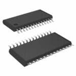 5T9050PGGI
The activity of extra discounts on wholesale prices is in full swing…
Please fill in your contact information and we will send you the latest wholesale price list.




