 ChipApex | Global Electronic Components Supplier
SEARCH
Search Product
Search Post
— IC芯片 | 连接器 | 传感器 | 被动器件 —
Search productSearch post
— IC芯片 | 连接器 | 传感器 | 被动器件 —
Consult the customer manager about the wholesale price.
consultation hotline:86-132-6715-2157
email:[email protected]
Contact the product manager for consultation. One-stop consultation is available.
Do you want a lower wholesale price? Please send us your inquiry and we will reply immediately.
The 5T9050PGGI8 is a clock fanout buffer manufactured by Renesas Electronics Corporation. It provides one input to five outputs distribution with a maximum frequency of 200 MHz. The device operates within a supply voltage range of 3 V to 3.6 V and functions across an industrial temperature range from -40°C to +85°C. It is housed in a 28-TSSOP package measuring 4.40 mm in width, designed for surface mount technology applications requiring precise clock signal distribution.
Verify the specific suffix 'PGGI8' against official Renesas documentation to ensure correct package type and tape-and-reel specifications. Confirm RoHS compliance status through current datasheets as regulatory requirements may evolve. Cross-reference the manufacturer part number with authorized distributor catalogs to validate authenticity and traceability before finalizing procurement orders.
Select this component when a single clock source requires expansion into five distinct output paths. Ensure the target application supports the specified 3 V to 3.6 V operating voltage range. Verify that the 200 MHz maximum frequency aligns with the system's timing requirements and that the 28-TSSOP footprint fits the printed circuit board layout constraints.
This part belongs to the family of clock buffer integrated circuits produced by Renesas Electronics. These components are engineered to maintain signal integrity while distributing timing references across multiple loads. The series typically addresses the needs of complex digital systems requiring synchronized clock signals derived from a single reference source.
Publicly confirmed substitute part numbers are not available in the provided documentation. Consult official Renesas cross-reference guides or authorized distributor databases for compatible alternatives if this specific model is unavailable.
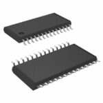 5T9050PGGI8
The activity of extra discounts on wholesale prices is in full swing…
Please fill in your contact information and we will send you the latest wholesale price list.





