 ChipApex | Global Electronic Components Supplier
SEARCH
Search Product
Search Post
— IC芯片 | 连接器 | 传感器 | 被动器件 —
Search productSearch post
— IC芯片 | 连接器 | 传感器 | 被动器件 —
Consult the customer manager about the wholesale price.
consultation hotline:86-132-6715-2157
email:[email protected]
Contact the product manager for consultation. One-stop consultation is available.
Do you want a lower wholesale price? Please send us your inquiry and we will reply immediately.
The 5T9304PGG8 is a low-jitter LVDS clock buffer manufactured by Renesas Electronics Corporation. It features a 2:4 fanout ratio, converting two differential inputs to four LVDS outputs with a maximum frequency of 450 MHz. The device operates on a supply voltage ranging from 2.3V to 2.7V and is housed in a 24-TSSOP package (0.173" width). It supports an operating temperature range of 0°C to 70°C and includes RoHS3 compliance.
Verify the specific suffix 'PGG8' against the official Renesas datasheet to confirm the exact package type and tape/reel specifications. Ensure the supply voltage requirements align with the 2.3V to 2.7V operational range. Confirm that the 24-TSSOP footprint matches the target PCB design constraints before finalizing procurement orders.
Select this component when a low-jitter LVDS buffer is required for distributing reference clocks to multiple FPGA or ASIC domains. The 2:4 fanout ratio makes it suitable for systems needing precise timing synchronization across different logic blocks. Ensure the application environment stays within the specified commercial temperature range and voltage limits.
This part belongs to the Terabuffer family of clock buffers designed for high-performance applications. It serves as a critical timing element in complex digital systems, ensuring signal integrity and minimal jitter during clock distribution. The device complements other clock generators and drivers in Renesas's portfolio for complete timing solutions.
Public sources indicate this product is no longer manufactured. Users should consult official Renesas documentation for verified substitute part numbers or alternative package types. Direct replacement verification is essential due to potential pinout or electrical specification differences in alternatives.
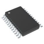 5T9304PGG8
The activity of extra discounts on wholesale prices is in full swing…
Please fill in your contact information and we will send you the latest wholesale price list.





