 ChipApex | Global Electronic Components Supplier
SEARCH
Search Product
Search Post
— IC芯片 | 连接器 | 传感器 | 被动器件 —
Search productSearch post
— IC芯片 | 连接器 | 传感器 | 被动器件 —
Consult the customer manager about the wholesale price.
consultation hotline:86-132-6715-2157
email:[email protected]
Contact the product manager for consultation. One-stop consultation is available.
Do you want a lower wholesale price? Please send us your inquiry and we will reply immediately.
The 5T93GL02PGGI is a 2.5V LVDS glitchless clock buffer from the Terabuffer II series by Renesas Electronics. It functions as a clock fanout buffer and distribution multiplexer IC, converting a single differential input into two LVDS outputs. The device supports frequencies up to 450 MHz and operates within an industrial temperature range of -40°C to 85°C. It is housed in a 20-TSSOP package with dimensions of 0.173 inches (4.40mm) width. This component is currently classified as obsolete.
This component is officially listed as obsolete by the manufacturer. Availability is limited to existing stock or third-party distributors. Verify authenticity and condition carefully when sourcing from non-authorized channels. Consider immediate design updates to incorporate replacement parts due to long-term supply risks associated with end-of-life status.
Select this part only if legacy compatibility with 2.5V LVDS interfaces is required. Ensure the 20-TSSOP footprint fits the PCB layout constraints. Evaluate thermal performance within the specified -40°C to 85°C range. Since it is obsolete, prioritize migration strategies to newer Renesas clock buffer families that offer similar glitchless differential-to-LVDS conversion capabilities.
The 5T93GL02PGGI belongs to the Terabuffer II family, designed for precise clock management. It serves as a specialized buffer for maintaining signal integrity in high-frequency environments. As an obsolete product, it represents an earlier generation of Renesas clock solutions before more advanced multi-output variants were introduced.
No direct public substitute part numbers are confirmed for this specific obsolete model. Designers should consult Renesas for current alternatives offering comparable 1:2 LVDS fanout functionality.
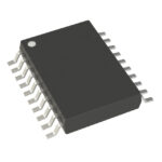 5T93GL02PGGI
The activity of extra discounts on wholesale prices is in full swing…
Please fill in your contact information and we will send you the latest wholesale price list.






