 ChipApex | Global Electronic Components Supplier
SEARCH
Search Product
Search Post
— IC芯片 | 连接器 | 传感器 | 被动器件 —
Search productSearch post
— IC芯片 | 连接器 | 传感器 | 被动器件 —
Consult the customer manager about the wholesale price.
consultation hotline:86-132-6715-2157
email:[email protected]
Contact the product manager for consultation. One-stop consultation is available.
Do you want a lower wholesale price? Please send us your inquiry and we will reply immediately.
The 5T93GL04PGGI is a 2.5V differential clock buffer manufactured by Renesas Electronics Corporation, designed for high-speed signal distribution in electronic systems. It functions as a 1:4 glitchless clock buffer, accepting a single differential input and providing four LVDS outputs with a maximum frequency of 450 MHz. The component is housed in a 24-TSSOP package, offering a compact form factor suitable for space-constrained applications. This device ensures precise timing integrity by eliminating glitches during output transitions, making it reliable for critical clock distribution networks where signal stability is paramount.
Verify the obsolete status of this specific part number before initiating any procurement process. Confirm availability through authorized distributors or check for direct replacements if new production units are required. Ensure that the 24-TSSOP package dimensions match your existing board layout constraints. Cross-reference the pinout configuration with current design schematics to prevent integration errors during replacement or upgrade scenarios.
Select this component when a 2.5V LVDS clock buffer with glitchless output transition is required. It is suitable for designs needing a single differential input expanded to four outputs without signal distortion. Consider the 450 MHz frequency limit and TSSOP package size relative to system speed and space requirements. Evaluate alternative packages if surface-mount constraints differ from standard TSSOP specifications.
This component belongs to Renesas' family of differential clock buffers and fanout devices. It complements other timing solutions by providing specialized LVDS output capabilities at 2.5V. The 5T93GL04 series offers variations in input/output configurations, serving diverse needs in high-speed digital circuits. Its design focuses on maintaining signal integrity across multiple branches in complex timing architectures.
Check for official substitute part numbers from Renesas or compatible vendors due to the obsolete status. Verify electrical compatibility including voltage levels, output types, and frequency ranges. Ensure pin-to-pin compatibility if direct replacement is intended to minimize redesign efforts.
The maximum operating frequency is 450 MHz.
Yes, it is designed as a glitchless clock buffer to ensure clean output transitions.
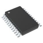 5T93GL04PGGI
The activity of extra discounts on wholesale prices is in full swing…
Please fill in your contact information and we will send you the latest wholesale price list.





