 ChipApex | Global Electronic Components Supplier
SEARCH
Search Product
Search Post
— IC芯片 | 连接器 | 传感器 | 被动器件 —
Search productSearch post
— IC芯片 | 连接器 | 传感器 | 被动器件 —
Consult the customer manager about the wholesale price.
consultation hotline:86-132-6715-2157
email:[email protected]
Contact the product manager for consultation. One-stop consultation is available.
Do you want a lower wholesale price? Please send us your inquiry and we will reply immediately.
The 5V2310PGG is a clock buffer integrated circuit manufactured by Renesas Electronics Corporation. It provides a single input to ten output fan-out buffering configuration with a maximum frequency of 200 MHz. The device operates on a supply voltage ranging from 2.3 V to 3.6 V and features LVTTL outputs. It is housed in a 24-TSSOP package with a width of 4.40 mm and supports surface-mount installation.
Verify component authenticity through authorized channels as the part status may be End-of-Life. Confirm package integrity and pin alignment against the 24-TSSOP specification before integration. Ensure supply voltage compatibility within the 2.3 V to 3.6 V range during system design validation.
Select this component when a single clock source requires expansion into ten distinct loads using LVTTL signaling. Evaluate thermal performance and board space constraints associated with the 24-TSSOP footprint. Consider alternative buffer families if differential signaling or lower power consumption is required.
This device belongs to the Renesas clock buffer family designed for signal integrity in digital systems. It serves as a critical interface between clock generators and multiple downstream receivers, ensuring synchronized data transmission across complex electronic assemblies.
Public confirmed substitutes include CDCVF2310PWR and CDCVF310PWR from Texas Instruments.
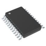 5V2310PGG
The activity of extra discounts on wholesale prices is in full swing…
Please fill in your contact information and we will send you the latest wholesale price list.





