 ChipApex | Global Electronic Components Supplier
SEARCH
Search Product
Search Post
— IC芯片 | 连接器 | 传感器 | 被动器件 —
Search productSearch post
— IC芯片 | 连接器 | 传感器 | 被动器件 —
Consult the customer manager about the wholesale price.
consultation hotline:86-132-6715-2157
email:[email protected]
Contact the product manager for consultation. One-stop consultation is available.
Do you want a lower wholesale price? Please send us your inquiry and we will reply immediately.
The 5V2310PGG8 is a high-performance clock buffer manufactured by Renesas Electronics Corporation. It operates with a maximum frequency of 200 MHz and provides a 1:10 input-to-output ratio. The device supports LVTTL input signaling and delivers LVCMOS output signals. It functions within a supply voltage range of 2.3 V to 3.6 V and is housed in a 24-TSSOP package with a width of 4.40 mm. The component is designed for surface mount installation and complies with RoHS3 standards.
Verify the specific suffix G8 against official Renesas documentation to confirm package type and tape/reel specifications. Confirm that the 24-TSSOP footprint matches the target PCB design. Check current status as this part may be subject to end-of-life notices or production changes documented in public product change notifications.
Select this component when a single clock source requires expansion into ten distinct paths. Ensure the system logic levels are compatible with LVTTL inputs and LVCMOS outputs. Verify that the operating temperature range meets the environmental requirements of the intended application.
This device belongs to the Renesas 5V23xx series of clock buffers. It is functionally related to other parts in the family, such as the 5V2310PGGI, which shares similar buffering characteristics but may differ in packaging or operational temperature ranges. The series targets general-purpose timing needs in consumer and industrial electronics.
Publicly confirmed direct substitutes include Texas Instruments CDCVF2310PWR and CDCVF310PWR. These alternatives offer comparable buffering functionality and should be evaluated for pin compatibility and electrical parameter alignment before integration.
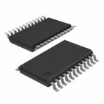 5V2310PGG8
The activity of extra discounts on wholesale prices is in full swing…
Please fill in your contact information and we will send you the latest wholesale price list.




