 ChipApex | Global Electronic Components Supplier
SEARCH
Search Product
Search Post
— IC芯片 | 连接器 | 传感器 | 被动器件 —
Search productSearch post
— IC芯片 | 连接器 | 传感器 | 被动器件 —
Consult the customer manager about the wholesale price.
consultation hotline:86-132-6715-2157
email:[email protected]
Contact the product manager for consultation. One-stop consultation is available.
Do you want a lower wholesale price? Please send us your inquiry and we will reply immediately.
The 5V2310PGGI is a clock fanout buffer manufactured by Renesas Electronics Corporation. It features a single circuit with a 1:10 input-to-output ratio, designed to distribute clock signals. The device supports a maximum frequency of 200 MHz and operates on a supply voltage ranging from 2.3 V to 3.6 V. It utilizes LVTTL output logic levels and accepts LVTTL inputs. The component is housed in a 24-TSSOP package with a width of 4.40 mm. It is rated for an operating temperature range of -40°C to +85°C and is intended for surface mount installation.
This component is scheduled for obsolescence and will be discontinued by the manufacturer. Current inventory may be limited or exhausted. Verify end-of-life status and availability through authorized distributors before finalizing design-in decisions. Consider alternative sourcing strategies due to impending discontinuation.
Select this component when a single-ended LVTTL clock source requires expansion into ten distinct outputs. Ensure the system power supply falls within the specified 2.3 V to 3.6 V range. Verify that the required clock frequency does not exceed 200 MHz. Confirm compatibility with the 24-TSSOP footprint during PCB layout planning.
The 5V2310 belongs to a family of clock buffer integrated circuits produced by Renesas. This specific variant focuses on high-speed fanout applications using standard logic levels. It serves as a critical timing element in systems requiring precise clock synchronization across multiple components without signal degradation.
Direct substitutes include CDCVF2310PWR and CDCVF310PWR from Texas Instruments. These alternatives offer similar functionality but require verification of pin compatibility and electrical specifications against the original design requirements.
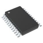 5V2310PGGI
The activity of extra discounts on wholesale prices is in full swing…
Please fill in your contact information and we will send you the latest wholesale price list.




