 ChipApex | Global Electronic Components Supplier
SEARCH
Search Product
Search Post
— IC芯片 | 连接器 | 传感器 | 被动器件 —
Search productSearch post
— IC芯片 | 连接器 | 传感器 | 被动器件 —
Consult the customer manager about the wholesale price.
consultation hotline:86-132-6715-2157
email:[email protected]
Contact the product manager for consultation. One-stop consultation is available.
Do you want a lower wholesale price? Please send us your inquiry and we will reply immediately.
The 5V41064NLGI is a single-output PCIe Gen1/2 clock synthesizer and jitter cleaner from Renesas Electronics. It operates with a maximum output frequency of 100 MHz and accepts a maximum input frequency of 25 MHz. The device utilizes HCSL output levels and is housed in a 16-pin QFN package. It functions within a supply voltage range of 3.135 V to 3.465 V and supports an operating temperature range of -40°C to +85°C.
Verify the specific suffix 'I' indicates the industrial temperature grade (-40°C to +85°C) compared to other variants. Confirm the 16-VFQFPN (3x3) package dimensions match your PCB footprint requirements. Ensure the HCSL output level compatibility aligns with the target receiver inputs. Check moisture sensitivity levels and reflow soldering profiles for assembly planning.
Select this component when a single differential or single-ended output is required for PCIe Gen1 or Gen2 interfaces. Consider the 100 MHz maximum output frequency limit against system timing needs. Evaluate the 25 MHz maximum input frequency constraint for reference clock sources. The compact 16-pin QFN package is suitable for space-constrained designs.
This part belongs to the 5V41064 series of clock synthesizers designed for high-speed serial interface applications. It serves as a specialized solution for generating clean clock signals for PCI Express standards. The series focuses on providing flexibility in system integration while maintaining signal integrity through jitter cleaning capabilities.
Public confirmed substitute part numbers are not available in the provided documentation.
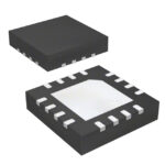 5V41064NLGI
The activity of extra discounts on wholesale prices is in full swing…
Please fill in your contact information and we will send you the latest wholesale price list.






