 ChipApex | Global Electronic Components Supplier
SEARCH
Search Product
Search Post
— IC芯片 | 连接器 | 传感器 | 被动器件 —
Search productSearch post
— IC芯片 | 连接器 | 传感器 | 被动器件 —
Consult the customer manager about the wholesale price.
consultation hotline:86-132-6715-2157
email:[email protected]
Contact the product manager for consultation. One-stop consultation is available.
Do you want a lower wholesale price? Please send us your inquiry and we will reply immediately.
The 5V41067APGG8 is a PCIe Gen2/3 compliant clock multiplexer and buffer manufactured by Renesas Electronics. It features a 2:4 differential input-to-output ratio, accepting two HCSL inputs and providing four outputs in HCSL or LVDS formats. The device operates at frequencies up to 200 MHz with a supply voltage range of 3.135V to 3.465V. Packaged in a 20-TSSOP (4.40mm wide) surface-mount housing, it supports an industrial operating temperature range from -40°C to +85°C. This component is designed for high-performance clock distribution in embedded systems requiring low jitter and EMI reduction.
The 5V41067A belongs to the 5V41067 family of clock drivers and distribution ICs. The 'PGG8' suffix indicates the specific package type (20-TSSOP) and tape-and-reel packaging configuration. This part is distinct from the tube-packaged 5V41067APGG variant.
The 5V41067APGGI is a pin-compatible alternative in a tube package. Note that the 5V41067APGGI has been marked as End-of-Life (EOL) with discontinuance notifications issued in March 2022. Verify current availability and RoHS compliance status when substituting.
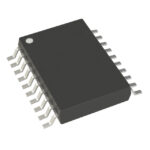 5V41067APGG8
The activity of extra discounts on wholesale prices is in full swing…
Please fill in your contact information and we will send you the latest wholesale price list.





