 ChipApex | Global Electronic Components Supplier
SEARCH
Search Product
Search Post
— IC芯片 | 连接器 | 传感器 | 被动器件 —
Search productSearch post
— IC芯片 | 连接器 | 传感器 | 被动器件 —
Consult the customer manager about the wholesale price.
consultation hotline:86-132-6715-2157
email:[email protected]
Contact the product manager for consultation. One-stop consultation is available.
Do you want a lower wholesale price? Please send us your inquiry and we will reply immediately.
The 5V41067APGGI is a clock multiplexer and buffer designed for PCI Express (PCIe) applications, manufactured by Renesas Electronics Corporation. It operates with a single supply voltage ranging from 3.135 V to 3.465 V and supports a maximum frequency of 200 MHz. The device features a 2:4 input-to-output ratio, accepting differential HCSL inputs and providing both HCSL and LVDS outputs. Packaged in a 20-TSSOP format, it functions within an industrial temperature range of -40°C to +85°C. This component serves as a critical signal distribution element in high-speed digital systems requiring precise clock routing.
The 5V41067APGGI belongs to the 5V41067 family of clock drivers and multiplexers. It is functionally related to variants such as the 5V41067APGG8, which shares similar electrical characteristics but differs in packaging configuration. The part is identified by aliases including IDT5V41067APGGI, reflecting its lineage within the integrated device technology portfolio now under Renesas.
Public documentation confirms the 5V41067APGG8 as a variant within the same product family. Verification of pin compatibility and specific package requirements (Tube vs. Reel/Cut Tape) is necessary before substitution.
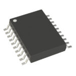 5V41067APGGI
The activity of extra discounts on wholesale prices is in full swing…
Please fill in your contact information and we will send you the latest wholesale price list.





