 ChipApex | Global Electronic Components Supplier
SEARCH
Search Product
Search Post
— IC芯片 | 连接器 | 传感器 | 被动器件 —
Search productSearch post
— IC芯片 | 连接器 | 传感器 | 被动器件 —
Consult the customer manager about the wholesale price.
consultation hotline:86-132-6715-2157
email:[email protected]
Contact the product manager for consultation. One-stop consultation is available.
Do you want a lower wholesale price? Please send us your inquiry and we will reply immediately.
The 5V41067APGGI8 is a PCIe clock multiplexer manufactured by Renesas Electronics Corporation. It functions as a 2-to-4 differential clock mux/buffer designed for PCI Express Gen2 and Gen3 applications. The device operates with a maximum frequency of 200MHz and accepts HCSL input signals, providing both HCSL and LVDS output signaling options. It is housed in a 20-TSSOP package with a width of 4.40mm. The component supports a supply voltage range of 3.135V to 3.465V and is rated for an operating temperature range of -40°C to 85°C.
The 5V41067APGGI8 part number indicates the reel packaging variant of the 5V41067A series. Distributors may list this under aliases such as IDT5V41067APGGI8. Verification of the specific suffix 'I8' against the manufacturer's official datasheet is required to confirm packaging details, as some sources associate the base model with tube packaging. Confirm RoHS3 compliance status directly from the current product documentation.
Select this component when a 2-input to 4-output differential clock multiplexer is required for PCIe interfaces. Ensure the design supports the specified 3.135V to 3.465V supply voltage. Verify that the target application can accommodate the 20-TSSOP footprint. Note that the broader 5V41067 family includes variants with different packaging or termination options; confirm the exact electrical characteristics match the board design requirements.
This component belongs to the 5V41067 family of PCIe clock drivers and multiplexers. It serves as a successor or alternative to earlier IDT clock distribution solutions. The device is part of Renesas' portfolio following the acquisition of IDT, maintaining compatibility with existing PCIe timing architectures while offering flexible output signaling formats.
Publicly confirmed substitute part numbers are not available in the provided data. Designers should consult the manufacturer's EOL notifications for recommended alternatives if sourcing is restricted.
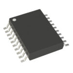 5V41067APGGI8
The activity of extra discounts on wholesale prices is in full swing…
Please fill in your contact information and we will send you the latest wholesale price list.






