 ChipApex | Global Electronic Components Supplier
SEARCH
Search Product
Search Post
— IC芯片 | 连接器 | 传感器 | 被动器件 —
Search productSearch post
— IC芯片 | 连接器 | 传感器 | 被动器件 —
Consult the customer manager about the wholesale price.
consultation hotline:86-132-6715-2157
email:[email protected]
Contact the product manager for consultation. One-stop consultation is available.
Do you want a lower wholesale price? Please send us your inquiry and we will reply immediately.
The Renesas 5V41234NLG is a single-output PCIe Gen2/3 compliant clock generator designed for spread spectrum operation. It features one differential HCSL output and operates within a supply voltage range of 3.135V to 3.465V. The device supports input frequencies from 100MHz to 200MHz, with an output frequency range of 100MHz to 200MHz. It utilizes a 16-VFQFPN (3x3) package with a bare pad, suitable for surface mount installation. The component functions as a PLL-based synthesizer to reduce electromagnetic interference in communication and embedded systems.
Verify the specific suffix 'NLG' against the manufacturer's current datasheet to confirm pinout and electrical specifications. Ensure compatibility with the required 16-VFQFPN footprint during PCB layout. Check for any Product Change Notifications (PCNs) related to assembly sites or material composition updates prior to procurement.
Select this component when a single differential HCSL output is required for PCIe applications. Confirm that the input crystal frequency matches the device's supported range. Verify that the system power supply aligns with the 3.135V to 3.465V operating window. Consider thermal dissipation requirements given the typical power consumption of 231mW.
The 5V41234NLG belongs to the IDT/Renesas 5V41235 family of PCIe clock synthesizers. It shares core functionality with variants like the 5V41235NLG8 but differs in output configuration. The 'NLG' suffix typically denotes the 16-VFQFPN package type. This part is distinct from buffer or distribution ICs in the same product line.
The 5V41235NLG8 is a closely related variant within the same family. Verify if the additional outputs or specific pin configurations of the 5V41235 series are compatible with the existing design before substitution.
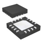 5V41234NLG
The activity of extra discounts on wholesale prices is in full swing…
Please fill in your contact information and we will send you the latest wholesale price list.





