 ChipApex | Global Electronic Components Supplier
SEARCH
Search Product
Search Post
— IC芯片 | 连接器 | 传感器 | 被动器件 —
Search productSearch post
— IC芯片 | 连接器 | 传感器 | 被动器件 —
Consult the customer manager about the wholesale price.
consultation hotline:86-132-6715-2157
email:[email protected]
Contact the product manager for consultation. One-stop consultation is available.
Do you want a lower wholesale price? Please send us your inquiry and we will reply immediately.
The IDT5V41234 is a single-output PCIe Gen1/Gen2/Gen3 compliant spread spectrum clock generator designed to reduce electromagnetic interference (EMI) in communication and embedded systems. It features one differential HCSL output with a frequency range of 100 MHz to 200 MHz, powered by a 3.3V supply. The device integrates a PLL for jitter cleaning and supports crystal inputs between 25 MHz and 25 MHz. Packaged in a compact 16-pin VFQFPN (3.0 x 3.0 mm) surface-mount format, it consumes approximately 231 mW of power and includes four differential termination resistors.
Verify the specific suffix 'G8' against the manufacturer's current datasheet to confirm package dimensions and lead finish specifications. Check for Product Change Notifications (PCNs) regarding assembly site changes or material updates. Ensure compatibility with the required 3.3V supply voltage and HCSL output signaling levels for the target application circuit.
Select this component when a single differential HCSL output is sufficient for the design. Compare against the 5V41235 model if two outputs are required instead of one. Verify that the input crystal frequency matches the 25 MHz requirement. Confirm that the 100-200 MHz output frequency range meets the system timing requirements.
This part belongs to the IDT 5V4123x family of PCIe clock synthesizers. It shares functional similarities with the 5V41235 but differs in output count. The device is manufactured by Renesas Electronics Corporation, having originated from Integrated Device Technology (IDT). It serves as a specialized timing solution for modern peripheral interfaces.
The 5V41235NLG8 is a related variant offering two outputs instead of one. Direct substitution requires verifying if the additional output is necessary or if the single output of the 5V41234 is sufficient for the PCB layout constraints.
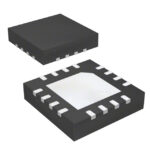 5V41234NLG8
The activity of extra discounts on wholesale prices is in full swing…
Please fill in your contact information and we will send you the latest wholesale price list.






