 ChipApex | Global Electronic Components Supplier
SEARCH
Search Product
Search Post
— IC芯片 | 连接器 | 传感器 | 被动器件 —
Search productSearch post
— IC芯片 | 连接器 | 传感器 | 被动器件 —
Consult the customer manager about the wholesale price.
consultation hotline:86-132-6715-2157
email:[email protected]
Contact the product manager for consultation. One-stop consultation is available.
Do you want a lower wholesale price? Please send us your inquiry and we will reply immediately.
The Renesas Electronics 621SDCGI8 is a low skew clock buffer from the 621S series, designed for high-speed signal distribution. It features one input and four outputs, supporting supply voltages between 1.8V and 3.3V. The device achieves a typical RMS jitter of 50fs and operates with a maximum input frequency of 200 MHz. Propagation delay is specified at a maximum of 4.5 ns. It functions within an industrial temperature range of -40°C to +105°C and is available in surface-mount packaging formats including cut tape and reel.
Verify component authenticity through authorized channels due to reported long delivery times and extended factory production cycles. Confirm package type availability, as the suffix '8' indicates specific reel or cut tape configurations distinct from tube packaging variants like the 621SDCGI. Ensure compliance with RoHS requirements prior to integration.
Select this model when low phase noise and precise timing alignment are critical for multi-output clock trees. Compare against the 651SDCGI8 for identical electrical performance but different packaging options. Consider the 553SDCGI8 if slightly lower propagation delay (4 ns) is required, noting it belongs to the 553S series.
This component belongs to the Renesas 621S family of clock buffers. It shares core specifications with the 651SDCGI8 but differs in standard packaging. The part number structure identifies the manufacturer, series, pin count, and package style, distinguishing it from other Renesas timing devices such as gate drivers or microcontrollers.
The 651SDCGI8 offers equivalent electrical characteristics and may serve as a functional substitute depending on packaging requirements. Verify pin compatibility and thermal performance before substitution.
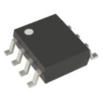 621SDCGI8
The activity of extra discounts on wholesale prices is in full swing…
Please fill in your contact information and we will send you the latest wholesale price list.







