 ChipApex | Global Electronic Components Supplier
SEARCH
Search Product
Search Post
— IC芯片 | 连接器 | 传感器 | 被动器件 —
Search productSearch post
— IC芯片 | 连接器 | 传感器 | 被动器件 —
Consult the customer manager about the wholesale price.
consultation hotline:86-132-6715-2157
email:[email protected]
Contact the product manager for consultation. One-stop consultation is available.
Do you want a lower wholesale price? Please send us your inquiry and we will reply immediately.
The Renesas Electronics 651MLF is a low skew clock buffer belonging to the 651 series. It features one input and four outputs, supporting LVCMOS logic levels for both input and output signals. The device operates within a supply voltage range of 1.425 V to 2.625 V and supports maximum input and output frequencies up to 200 MHz. Maximum propagation delay is specified at 5 ns. It is housed in an SOIC-8 surface-mount package and functions within an operating temperature range of -40°C to +85°C.
The 651MLF is identified as a discontinued product by the manufacturer. Verification of availability requires checking secondary market distributors or surplus suppliers. Designers should confirm end-of-life status and plan for component obsolescence management. Sourcing may involve long lead times or limited stock from third-party vendors rather than direct manufacturer allocation.
Select this component when a low skew, 1-to-4 LVCMOS clock buffer is required for frequencies up to 200 MHz. Ensure the system power supply falls within the 1.425 V to 2.625 V range. The SOIC-8 package must be compatible with the PCB footprint. Due to its discontinued status, evaluate alternative components from current production lines that match these electrical specifications.
The 651MLF is part of the Renesas 651 series of clock buffers. This series is designed for applications requiring precise timing and low skew distribution. It serves as a legacy component within the Renesas portfolio, often replaced by newer generations in modern designs. The 'M' suffix typically denotes the SOIC-8 package variant.
As the 651MLF is discontinued, verify functional equivalents from current Renesas clock buffer lines. Check for pin compatibility with the SOIC-8 package and ensure voltage ranges (1.425V–2.625V) and frequency limits (200MHz) are met by potential substitutes.
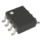 651MLF
The activity of extra discounts on wholesale prices is in full swing…
Please fill in your contact information and we will send you the latest wholesale price list.





