 ChipApex | Global Electronic Components Supplier
SEARCH
Search Product
Search Post
— IC芯片 | 连接器 | 传感器 | 被动器件 —
Search productSearch post
— IC芯片 | 连接器 | 传感器 | 被动器件 —
Consult the customer manager about the wholesale price.
consultation hotline:86-132-6715-2157
email:[email protected]
Contact the product manager for consultation. One-stop consultation is available.
Do you want a lower wholesale price? Please send us your inquiry and we will reply immediately.
The Renesas 651SCMGI is a single-input to four-output LVCMOS clock buffer IC designed for low skew applications. It operates within a supply voltage range of 1.71V to 3.465V, supporting three distinct voltage domains: 1.8V (1.71V–1.89V), 2.5V (2.375V–2.625V), and 3.3V (3.135V–3.465V). The device supports maximum input frequencies up to 200 MHz with a maximum propagation delay of 4.5 ns. It is housed in an 8-UFDFN package (8-VFQFN, 2x2 mm) and functions across an operating temperature range of -40°C to 105°C.
Verify the specific suffix against the manufacturer's current documentation, as the '651SCMGI' designation may correspond to tube or reel packaging variants. Confirm availability status directly with authorized distributors, as stock levels fluctuate. Ensure the selected variant matches the required packaging quantity and moisture sensitivity level specifications for the intended assembly process.
Select this component when a single-ended LVCMOS input must drive four separate loads with minimal skew. Verify that the system power rails align with the specified 1.8V, 2.5V, or 3.3V operating ranges. Ensure the PCB layout accommodates the 2x2 mm 8-VFQFN footprint and that thermal requirements are met within the -40°C to 105°C ambient temperature range.
This part belongs to the 651S series of clock buffers. It serves as a foundational component for timing distribution in digital systems. Related variants include the 651SCMGI8, which shares identical electrical characteristics but differs in standard shipping packaging (reel vs. tube/other).
The 651SCMGI8 is a parameter-equivalent alternative from Renesas Electronics Corporation. It offers identical electrical specifications and pinout compatibility, differing primarily in packaging format.
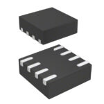 651SCMGI
The activity of extra discounts on wholesale prices is in full swing…
Please fill in your contact information and we will send you the latest wholesale price list.





