 ChipApex | Global Electronic Components Supplier
SEARCH
Search Product
Search Post
— IC芯片 | 连接器 | 传感器 | 被动器件 —
Search productSearch post
— IC芯片 | 连接器 | 传感器 | 被动器件 —
Consult the customer manager about the wholesale price.
consultation hotline:86-132-6715-2157
email:[email protected]
Contact the product manager for consultation. One-stop consultation is available.
Do you want a lower wholesale price? Please send us your inquiry and we will reply immediately.
The Renesas Electronics Corporation 651SCMGI8 is a single-input to four-output LVCMOS clock buffer within the 651S series. It supports maximum input frequencies up to 200 MHz with a typical propagation delay of 4.5 ns. The device operates across three voltage ranges: 1.71V–1.89V, 2.375V–2.625V, and 3.135V–3.465V. Packaged in an 8-UFDFN (2x2 mm) surface-mount format, it functions reliably between -40°C and +105°C ambient temperature. The component features low skew characteristics and sub-50fs RMS additive phase jitter.
Verify the manufacturer part number 651SCMGI8 against official Renesas documentation before procurement. Confirm that the 8-VFQFN package dimensions match the design footprint. Ensure supply chain sources provide RoHS3 compliance certificates as specified in the datasheet. Check for any recent Product Change Notices regarding labeling or assembly location updates.
Select this component when low jitter and high-frequency operation are required for LVCMOS loads. The 651SCMGI8 is suitable for designs needing a single source to drive multiple synchronous components. Verify that the PCB layout accommodates the 2x2 mm UFDFN package. Consider thermal dissipation requirements if operating at the upper limit of the 105°C temperature range.
The 651SCMGI8 belongs to the 651S family of clock buffers designed for cost-effective, high-speed applications. It serves as a replacement for older discrete logic solutions in timing networks. The device complements other Renesas timing products like the 553S and 524S series by offering specific jitter performance metrics.
The 524SCMGI8 is listed as a parameter-equivalent alternative from Renesas Electronics Corporation.
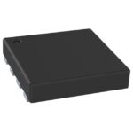 651SCMGI8
The activity of extra discounts on wholesale prices is in full swing…
Please fill in your contact information and we will send you the latest wholesale price list.





