 ChipApex | Global Electronic Components Supplier
SEARCH
Search Product
Search Post
— IC芯片 | 连接器 | 传感器 | 被动器件 —
Search productSearch post
— IC芯片 | 连接器 | 传感器 | 被动器件 —
Consult the customer manager about the wholesale price.
consultation hotline:86-132-6715-2157
email:[email protected]
Contact the product manager for consultation. One-stop consultation is available.
Do you want a lower wholesale price? Please send us your inquiry and we will reply immediately.
The Texas Instruments 66AK2G12ABY60 is a multicore System-on-Chip (SoC) based on the Keystone II architecture, integrating one Arm Cortex-A15 core and one C66x DSP core. Both processors operate at up to 1000 MHz. The device features extensive error correction code (ECC) protection for L1/L2 memory and shared SRAM. It includes two PRU-ICSS subsystems, a Gigabit Ethernet MAC with IEEE 1588v2 support, and a single-lane PCIe Gen 2 interface. Memory interfaces include DDR3L EMIF supporting up to 4 GB and QSPI. The component is housed in a 625-ball FCBGA package.
Verify the specific speed grade suffix associated with the ABY60 designation against the official datasheet to confirm clock frequency capabilities. Ensure that the ordering information matches the required industrial temperature range specifications. Confirm package availability and lead times through authorized distribution channels prior to procurement planning.
Select this SoC for applications requiring simultaneous real-time DSP processing and high-level OS execution. The integrated PRU-ICSS modules are suitable for deterministic control tasks. Designers must account for the 625-ball FCBGA package requirements during PCB layout. Verify power supply sequencing for the multiple voltage domains, including DVDD_DDR and DVDD18, as specified in the electrical characteristics.
This component belongs to the 66AK2G1x family of multicore DSP+Arm KeyStone II SoCs. It shares the same architectural foundation as other devices in the series but differs in specific feature sets and performance grades. The ABY package denotes the 625-ball plastic ball grid array form factor used across several variants in this product line.
Consult the device comparison table in the datasheet for compatible alternatives within the 66AK2G1x family. Verify pin-to-pin compatibility and feature parity before substituting with other members of the series.
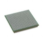 66AK2G12ABY60
The activity of extra discounts on wholesale prices is in full swing…
Please fill in your contact information and we will send you the latest wholesale price list.






