 ChipApex | Global Electronic Components Supplier
71T75802S150BGG8
Search Product
Search Post
— IC芯片 | 连接器 | 传感器 | 被动器件 —
Search productSearch post
— IC芯片 | 连接器 | 传感器 | 被动器件 —
Consult the customer manager about the wholesale price.
consultation hotline:86-132-6715-2157
email:[email protected]
Contact the product manager for consultation. One-stop consultation is available.
Do you want a lower wholesale price? Please send us your inquiry and we will reply immediately.
The Renesas Electronics Corporation 71T75802S150BGG8 is a 18 Mbit synchronous static random access memory (SRAM) device organized as 1M x 18. It utilizes Zero Bus Turnaround (ZBT) technology to eliminate dead cycles between read and write operations, supporting a maximum clock frequency of 150 MHz with a 3.8 ns access time. The component operates on a 2.5V core voltage supply within a range of 2.375V to 2.625V. It is housed in a 119-pin plastic ball grid array (PBGA) package measuring 14x22 mm and supports an operating temperature range of 0°C to 70°C.
Verify component authenticity through authorized channels due to discontinuation status. Confirm package integrity and moisture sensitivity level handling procedures prior to assembly. Cross-reference datasheet revisions to ensure compatibility with existing design specifications. Validate RoHS compliance status against specific project regulatory requirements before procurement finalization.
Select this component when system architecture requires 18-bit data width and synchronous parallel interface capabilities. Ensure voltage supply constraints align with the specified 2.375V to 2.625V range. Consider thermal management solutions suitable for the 0°C to 70°C industrial temperature grade. Evaluate PCB layout requirements for the 119-pin PBGA footprint during initial design phases.
This part belongs to the 71T75802 family of high-performance synchronous SRAMs. The series offers various speed grades and packaging options to accommodate different system timing and physical space constraints. All variants share the same fundamental ZBT architecture and 1M x 18 organization, differing primarily in clock frequency limits and thermal ratings.
Publicly confirmed substitute part numbers are not available in verified documentation. Consult manufacturer obsolescence notices for potential end-of-life management strategies or approved alternative components within the same product family.
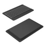 71T75802S150BGG8
The activity of extra discounts on wholesale prices is in full swing…
Please fill in your contact information and we will send you the latest wholesale price list.





