 ChipApex | Global Electronic Components Supplier
SEARCH
Search Product
Search Post
— IC芯片 | 连接器 | 传感器 | 被动器件 —
Search productSearch post
— IC芯片 | 连接器 | 传感器 | 被动器件 —
Consult the customer manager about the wholesale price.
consultation hotline:86-132-6715-2157
email:[email protected]
Contact the product manager for consultation. One-stop consultation is available.
Do you want a lower wholesale price? Please send us your inquiry and we will reply immediately.
The Renesas Electronics Corporation 7201LA15J is an asynchronous FIFO memory device with a storage capacity of 4.5K bits, organized as 512 words by 9 bits. It operates within a supply voltage range of 4.5 V to 5.5 V and supports data rates up to 40 MHz with a maximum access time of 15 ns. The component utilizes a unidirectional bus architecture and is housed in a 32-PLCC package measuring 14x11.46 mm. Designed for surface mount installation, it functions reliably across a commercial temperature range of 0°C to 70°C.
Verify the exact suffix designation against official Renesas documentation, as variations such as JGI8 or J8 may indicate differences in packaging or RoHS compliance status. Confirm current availability and lifecycle status directly with authorized distributors, as this component series may be subject to discontinuation notices. Ensure that the required moisture sensitivity level and reflow soldering profiles align with your manufacturing capabilities before placing orders.
Select this component when a 512x9 word depth is required for asynchronous data buffering applications. The 15 ns access time and 40 MHz speed suit moderate-speed digital interfaces. Consider the 32-PLCC package constraints for PCB layout. Verify that the 4.5 V to 5.5 V supply voltage matches your system's power rails. Evaluate if the unidirectional bus direction meets your specific data flow needs without requiring additional logic inversion.
This part belongs to the Renesas 7201L series of CMOS parallel FIFOs. The series typically includes variants with different access times and package options, such as the 7201LA12 for faster performance or other pin-compatible forms. These components are designed for general-purpose memory buffering in industrial and commercial electronic equipment, providing reliable data integrity through standard CMOS logic levels.
Check for direct replacements like the IDT7201LA15J or other 7201L series variants with matching electrical specifications. Ensure any substitute maintains the 512x9 organization and 32-PLCC footprint. Verify compatibility with existing firmware or hardware control signals before implementation.
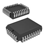 7201LA15J
The activity of extra discounts on wholesale prices is in full swing…
Please fill in your contact information and we will send you the latest wholesale price list.






