 ChipApex | Global Electronic Components Supplier
SEARCH
Search Product
Search Post
— IC芯片 | 连接器 | 传感器 | 被动器件 —
Search productSearch post
— IC芯片 | 连接器 | 传感器 | 被动器件 —
Consult the customer manager about the wholesale price.
consultation hotline:86-132-6715-2157
email:[email protected]
Contact the product manager for consultation. One-stop consultation is available.
Do you want a lower wholesale price? Please send us your inquiry and we will reply immediately.
The Renesas 7202LA20J8 is an asynchronous FIFO memory device with a storage capacity of 9K bits, organized as 1K words by 9 bits. It operates at a maximum data rate of 33.3MHz with a 20ns access time. The component supports unidirectional bus direction and functions within a supply voltage range of 4.5V to 5.5V. Maximum supply current is specified at 80mA. It is housed in a 32-PLCC package (14x11.46mm) and operates within a commercial temperature range of 0°C to 70°C.
Verify the specific suffix J8 confirms the 32-PLCC package and lead type. Confirm RoHS compliance status as some variants may be non-compliant. Check for end-of-life notices or obsolescence warnings from Renesas. Ensure the 9-bit width matches system requirements, as standard widths are often 8 or 10 bits. Validate operating temperature range against environmental constraints.
Select this part when a 9-bit wide asynchronous buffer is required. The 1K depth provides moderate storage for burst data handling. Verify that the 33.3MHz speed meets system timing requirements. Consider the 32-PLCC package for surface mount assembly compatibility. Compare power consumption against other FIFO options if battery life is critical.
This component belongs to the Renesas 7200 series of asynchronous FIFOs. It shares architectural similarities with other parts in the family but differs in memory depth and speed grades. The 7202 variant specifically targets applications requiring 1K x 9 organization. It is distinct from SRAM devices like the 7134 series which offer dual-port access.
IDT7202LA20J8 is a documented alias for this component. Cross-reference pinouts and electrical specifications before substitution. Verify package dimensions match existing PCB footprints.
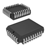 7202LA20J8
The activity of extra discounts on wholesale prices is in full swing…
Please fill in your contact information and we will send you the latest wholesale price list.






