 ChipApex | Global Electronic Components Supplier
SEARCH
Search Product
Search Post
— IC芯片 | 连接器 | 传感器 | 被动器件 —
Search productSearch post
— IC芯片 | 连接器 | 传感器 | 被动器件 —
Consult the customer manager about the wholesale price.
consultation hotline:86-132-6715-2157
email:[email protected]
Contact the product manager for consultation. One-stop consultation is available.
Do you want a lower wholesale price? Please send us your inquiry and we will reply immediately.
The Renesas 72255LA10TFG8 is a SuperSync synchronous FIFO memory device featuring an 8K x 18-bit architecture and a total storage capacity of 144K bits. It operates with a data rate of 100MHz and an access time of 8ns, supporting full-width first-word fall-through (FWFT) and retransmit capabilities. The component functions within a core voltage range of 4V to 5.5V, drawing a maximum supply current of 80mA. It is housed in a 64-LQFP surface-mount package and supports uni-directional bus architecture.
Verify the specific suffix 'FG8' corresponds to the 64-LQFP package variant when sourcing. Confirm RoHS3 compliance status as per the latest manufacturer documentation. Ensure the operating voltage range aligns with the system's 4V to 5.5V requirement. Check for any recent Product Change Notifications (PCN) regarding assembly facilities or labeling changes that may affect qualification.
Select this component for applications requiring high-speed synchronous data transfer with 18-bit word width. The 8ns access time and 100MHz data rate suit demanding throughput requirements. Consider the FWFT feature if low-latency data retrieval is critical. Ensure the 64-pin LQFP footprint fits the PCB layout constraints compared to other pin-count options in the 72V series.
This part belongs to the Renesas 72V261/72255 SuperSync family of synchronous FIFOs. It shares architectural similarities with other members like the 72V261LA10TFG8 but differs in depth and width specifications. The 72255LA10TFG8 specifically targets 5V logic interfaces with its wider 18-bit data path, distinguishing it from narrower 8-bit or 9-bit variants in the same series.
The 72255LA10TFG8 serves as a direct functional substitute for the obsolete 72255LA20TFI8. Both parts maintain identical 144K (8Kx18) capacity and electrical characteristics. Verify package compatibility when replacing the older TFI8 suffix with the current FGF8 designation.
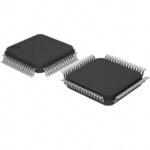 72255LA10TFG8
The activity of extra discounts on wholesale prices is in full swing…
Please fill in your contact information and we will send you the latest wholesale price list.







