 ChipApex | Global Electronic Components Supplier
74ABT00PW,118
Search Product
Search Post
— IC芯片 | 连接器 | 传感器 | 被动器件 —
Search productSearch post
— IC芯片 | 连接器 | 传感器 | 被动器件 —
Consult the customer manager about the wholesale price.
consultation hotline:86-132-6715-2157
email:[email protected]
Contact the product manager for consultation. One-stop consultation is available.
Do you want a lower wholesale price? Please send us your inquiry and we will reply immediately.
The Nexperia 74ABT00PW,118 is a quad 2-input NAND gate in a TSSOP14 package. It operates on a supply voltage of 4.5 V to 5.5 V with BiCMOS technology for high speed and output drive. Key electrical parameters include a low-level output current of 20 mA and a high-level output current of -15 mA. Propagation delays range from 1.0 ns to 4.1 ns at 5.0 V. The device supports partial power-down via IOFF circuitry and withstands latch-up currents exceeding 500 mA.
Verify the specific ordering suffix
Select this component when designing 5V logic systems requiring fast switching speeds and robust noise immunity. The BiCMOS architecture offers superior drive strength compared to standard CMOS alternatives. Ensure the design accommodates the 4.5 V to 5.5 V supply range and utilizes the IOFF feature if partial power management is required for the target application.
This part belongs to the 74ABT series, which utilizes Bipolar-CMOS technology to achieve performance levels between standard 74HC and 74F families. The PW suffix indicates a plastic thin shrink small outline package (TSSOP14), suitable for surface-mount assembly where space efficiency is prioritized alongside high-density circuit board layouts.
Check for 74ABT00D as an alternative SO14 package version from the same manufacturer. Verify pinout compatibility before substituting with other quad NAND gates from different logic families.
The IOFF circuitry disables the outputs when the device is powered down, preventing potentially damaging backflow current through the device during partial power-down applications.
The device exceeds 500 mA per JESD78B Class II Level A for latch-up protection.
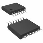 74ABT00PW,118
The activity of extra discounts on wholesale prices is in full swing…
Please fill in your contact information and we will send you the latest wholesale price list.




