 ChipApex | Global Electronic Components Supplier

SEARCH
Search Product
Search Post
— IC芯片 | 连接器 | 传感器 | 被动器件 —
Search productSearch post
— IC芯片 | 连接器 | 传感器 | 被动器件 —
Consult the customer manager about the wholesale price.
consultation hotline:86-132-6715-2157
email:[email protected]
Contact the product manager for consultation. One-stop consultation is available.
Do you want a lower wholesale price? Please send us your inquiry and we will reply immediately.
74ABT16240ADGG,118 is listed in the Buffers, Drivers, Receivers, Transceivers range at ChipApex. The manufacturer field lists Nexperia USA Inc.. Its product description is IC BUFFER INVERT 5.5V 48TSSOP. Review the specifications below when checking this part for your BOM.
The Nexperia 74ABT16240ADGG,118 is a 16-bit inverting buffer and line driver featuring 3-state outputs. It operates within a supply voltage range of 4.5 V to 5.5 V. The device provides an output drive capability of +64 mA for low-level states and -32 mA for high-level states. Propagation delays are specified between 1.0 ns and 3.7 ns at 5.0 V. It utilizes a TSSOP48 package (SOT362-1) and supports operation from -40 °C to +85 °C.
Verify the specific ordering suffix
Select this component when designing 5 V logic interfaces requiring high drive strength and fast propagation speeds. Ensure the application environment remains within the specified -40 °C to +85 °C temperature range. Confirm that the system architecture accommodates the four independent output enable signals required to control the 3-state buffers effectively.
This device belongs to the 74ABT series, which utilizes BiCMOS technology to deliver higher speed and drive capability compared to standard CMOS or LVC families. It is designed specifically for 5 V applications, distinguishing it from lower voltage logic families like LVC or AUP. The 16-bit configuration allows for efficient parallel data transmission in wide-bus architectures.
Check for the 74ABT16240ADL variant if an SSOP48 package is required instead of the TSSOP48 used by the ADGG suffix. Verify pinout compatibility before substitution.
The integrated IOFF circuitry automatically disables the outputs, preventing potentially damaging backflow current through the device when it is powered down.
The multiple VCC and GND pins are included to minimize switching noise within the circuit.
Explore related parts through Logic, Integrated Circuits (ICs), all product categories, ChipApex homepage.
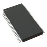 74ABT16240ADGG,118

The activity of extra discounts on wholesale prices is in full swing…
Please fill in your contact information and we will send you the latest wholesale price list.





