 ChipApex | Global Electronic Components Supplier

SEARCH
Search Product
Search Post
— IC芯片 | 连接器 | 传感器 | 被动器件 —
Search productSearch post
— IC芯片 | 连接器 | 传感器 | 被动器件 —
Consult the customer manager about the wholesale price.
consultation hotline:86-132-6715-2157
email:[email protected]
Contact the product manager for consultation. One-stop consultation is available.
Do you want a lower wholesale price? Please send us your inquiry and we will reply immediately.
74ABT241CSJX is listed in the Buffers, Drivers, Receivers, Transceivers range at ChipApex. The manufacturer field lists onsemi. Its product description is IC BUFF NON-INVERT 5.5V 20SOP. Review the specifications below when checking this part for your BOM.
The onsemi 74ABT241CSJX is an octal buffer and line driver with 3-STATE outputs, manufactured by Fairchild Semiconductor. It operates within a supply voltage range of +4.5V to +5.5V and supports ambient temperatures from -40°C to +85°C. The device features non-inverting buffers with output sink capability of 64 mA and source capability of 32 mA. Propagation delay is typically 4.6 ns at VCC = 5V with CL = 50 pF. Input HIGH voltage is recognized at 2.0 V minimum, while input LOW is recognized at 0.8 V maximum. Output HIGH voltage is 2.0 V minimum at IOH = -32 mA, and output LOW voltage is 0.55 V maximum at IOL = 64 mA.
Verify the component status as discontinued or obsolete through official manufacturer channels before procurement planning. Confirm that the 'X' suffix denotes tape and reel packaging if required for automated assembly processes. Ensure compatibility with existing board layouts utilizing the 20-Lead Small Outline Package (SOP) format specified in the datasheet.
Select this component when high drive current capabilities are necessary for bus driving applications. The ABT logic family provides faster propagation delays compared to standard ALS series devices. Verify that the system environment remains within the recommended operating conditions regarding supply voltage and ambient temperature limits to ensure reliable performance.
This part belongs to the 74ABT logic family, known for high-speed operation and compatibility with TTL inputs. Manufactured originally by Fairchild Semiconductor, it serves as an octal buffer suitable for high-performance digital systems requiring robust signal integrity and bus isolation capabilities.
Consult official manufacturer documentation for verified substitute part numbers. Cross-reference pinouts and electrical characteristics carefully when considering alternative vendors or updated revisions of the same logic family.
OE1 and OE2 are output enable inputs that control the 3-state outputs. OE1 is active LOW, while OE2 is active HIGH, allowing flexible control over the upper and lower halves of the octal bus.
The device maintains high impedance glitch-free bus loading throughout the entire power-up and power-down cycle, preventing unintended signal transitions during voltage transitions.
Explore related parts through Logic, Integrated Circuits (ICs), all product categories, ChipApex homepage.
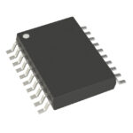 74ABT241CSJX

The activity of extra discounts on wholesale prices is in full swing…
Please fill in your contact information and we will send you the latest wholesale price list.





