 ChipApex | Global Electronic Components Supplier
SEARCH
Search Product
Search Post
— IC芯片 | 连接器 | 传感器 | 被动器件 —
Search productSearch post
— IC芯片 | 连接器 | 传感器 | 被动器件 —
Consult the customer manager about the wholesale price.
consultation hotline:86-132-6715-2157
email:[email protected]
Contact the product manager for consultation. One-stop consultation is available.
Do you want a lower wholesale price? Please send us your inquiry and we will reply immediately.
The NXP USA Inc. 74ABT373AN,112 is an octal transparent latch featuring 3-State output buffers, manufactured by Philips Semiconductors and distributed by NXP. It operates within a DC supply voltage range of 4.5V to 5.5V and supports an operating temperature range from -40°C to +85°C. The device provides high-speed performance with propagation delays (Dn to Qn) typically ranging from 1.4ns to 4.7ns at VCC = 5V. It offers robust output drive capabilities of +64mA/-32mA and includes power-up 3-State functionality to permit live insertion or extraction.
Verify the specific package type required, as the 74ABT373A series is available in multiple configurations including 20-Pin Plastic DIP, SO, SSOP Type II, and TSSOP Type I. Confirm that the 'N' suffix corresponds to the desired plastic DIP package variant when sourcing replacements. Ensure compatibility with the specified 4.5V to 5.5V supply voltage range and -40°C to +85°C operating temperature limits for your application environment.
Select this component for applications requiring octal data latching with high-speed BiCMOS performance. It is suitable where strong output drive currents are necessary to maintain signal integrity on heavy loads. Consider the 3-State feature if bus sharing is required. Verify that the 20-pin package format fits the PCB layout constraints and that the logic levels align with the 4.5V to 5.5V VCC requirements.
This part belongs to the 74ABT373A family of octal transparent latches. It is a high-performance BiCMOS device combining low static and dynamic power dissipation with high speed. The product specification was originally published by Philips Semiconductors in February 1995. The 'N' designation specifically identifies the 20-Pin Plastic DIP package version within the broader 74ABT373A product line.
Compatible substitutes include other 74ABT373A variants with different packages such as 74ABT373AD (SO), 74ABT373ADB (SSOP), or 74ABT373APW (TSSOP). Ensure the replacement maintains the same 20-pin configuration and electrical characteristics if pinout compatibility is critical.
The active-Low Output Enable (OE) pin controls all eight 3-State buffers independently of the latch operation. When OE is Low, data appears at the outputs; when High, the outputs enter a high-impedance 'OFF' state.
The Power-up 3-State feature ensures that outputs are in a high-impedance state during power-up, permitting live insertion or extraction without interfering with other devices on the bus.
At VCC = 5V and CL = 50pF, the typical propagation delay from Dn to Qn is 3.2ns for tPLH and 3.6ns for tPHL.
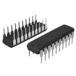 74ABT373AN,112
The activity of extra discounts on wholesale prices is in full swing…
Please fill in your contact information and we will send you the latest wholesale price list.





