 ChipApex | Global Electronic Components Supplier
SEARCH
Search Product
Search Post
— IC芯片 | 连接器 | 传感器 | 被动器件 —
Search productSearch post
— IC芯片 | 连接器 | 传感器 | 被动器件 —
Consult the customer manager about the wholesale price.
consultation hotline:86-132-6715-2157
email:[email protected]
Contact the product manager for consultation. One-stop consultation is available.
Do you want a lower wholesale price? Please send us your inquiry and we will reply immediately.
The onsemi 74ACT299SC is an 8-bit universal shift/storage register featuring common parallel I/O pins and 3-STATE outputs. It supports four operating modes: hold, shift left, shift right, and parallel load. The device operates within a supply voltage range of 4.5V to 5.0V and includes TTL-compatible inputs. Key electrical parameters include a maximum propagation delay of 14.0ns at 5.0V with 50pF load, output current capability of ±24mA, and quiescent supply current of 40µA. It is housed in a 20-lead SOIC package.
Verify the specific ordering suffix to confirm the package type, as the base part number applies to multiple packages including SOIC, TSSOP, and PDIP. Confirm that the 'X' suffix is required if tape and reel packaging is needed rather than standard tube or tray. Ensure the design accounts for the ACT logic family voltage requirements.
Select this component when an 8-bit universal shift register with shared I/O pins is required to minimize footprint. The ACT series provides TTL-compatible input thresholds while maintaining CMOS performance. Consider the 3-STATE output capability for bus sharing applications. Verify that the 4.5V to 5.0V supply range aligns with the system power architecture.
The 74ACT299 belongs to the AC/ACT logic family, which offers high-speed operation with low power consumption. This specific variant is the ACT version, optimized for 5V operation with TTL-compatible inputs. It serves as a versatile digital storage element capable of handling complex shifting and loading operations within a single integrated circuit package.
Direct substitutes include the 74AC299SC for AC logic family compatibility and the MC74ACT299SC from the same manufacturer. Cross-brand equivalents such as the SN74ACT299N are available but require verification of pinout and electrical specifications against the original datasheet.
Parallel data is loaded by setting mode select inputs S0 and S1 to HIGH. The data present on the I/O pins is transferred to the flip-flops on the rising edge of the clock pulse.
The MR pin provides an asynchronous reset. A LOW signal on MR overrides all other inputs and forces all flip-flop outputs to a LOW state immediately.
Yes. Applying a HIGH signal to either OE1 or OE2 disables the 3-STATE buffers, placing the I/O pins in a high-impedance state without affecting the internal shift or storage operations.
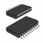 74ACT299SC
The activity of extra discounts on wholesale prices is in full swing…
Please fill in your contact information and we will send you the latest wholesale price list.






